


Samsung's second wafer fab in the United States plans to produce HBM basic wafers for AMD and other companies
According to the South Korean media Daily Economy, Samsung Electronics' wafer foundry business plans to produce the base die required for high bandwidth memory (HBM) for customers such as AMD at its second wafer fab in the Taylor City cluster in Texas, USA. In addition to supplying AMD, related products may also be used in the AI application specific integrated circuits (ASICs) created by Broadcom for customers in the future.
According to the plan, the first wafer fab of Samsung's wafer foundry Taylor Cluster will be put into operation within 2026, and the second wafer fab is expected to start construction this month and be put into operation in 2030. If the relevant plans proceed smoothly, Taylor's production base will not only undertake advanced logic chip manufacturing tasks, but also have the potential to further participate in the production of AI memory core components, becoming an important manufacturing node for Samsung to connect wafer foundry, memory, and high-performance computing businesses.
HBM provides high bandwidth and large capacity in a limited space by vertically stacking multi-layer storage chips, and is an important component of AI accelerators and high-performance computing systems. The basic bare chip is located at the bottom of the HBM stack and is responsible for communication between the storage stack and computing chips such as XPU. Although its name is not as eye-catching as storage chips or computing chips, with the increasing requirements for transmission speed, power consumption, and system synergy, the design and manufacturing level of basic bare chips is becoming increasingly critical.
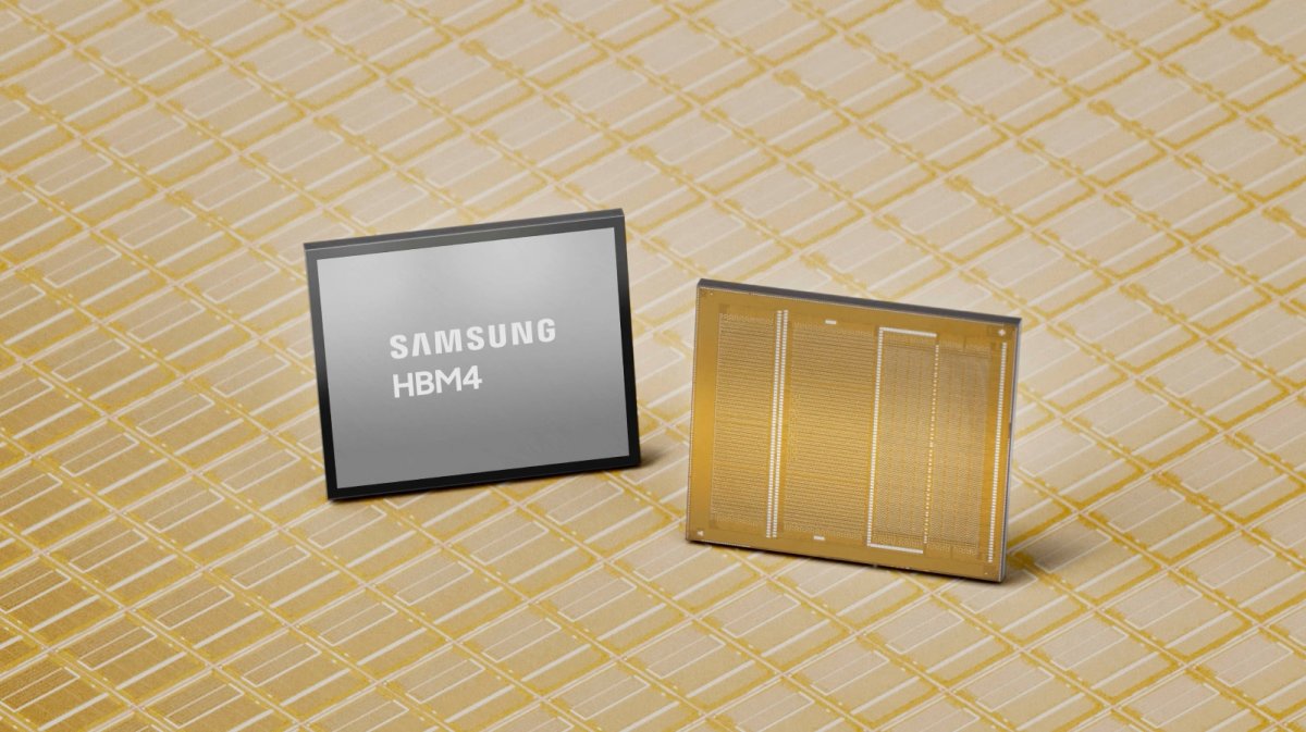
At present, Samsung's wafer foundry mainly supplies HBM basic wafers to Samsung's own memory business. However, starting from the HBM4 generation, the industry's demand for basic die performance has further increased, and memory manufacturers using their own processes have gradually become difficult to meet the demand. Especially in terms of data transmission efficiency, interface complexity, and advanced process adaptation, the advanced manufacturing capabilities possessed by external wafer foundry companies are beginning to show value.
At the same time, the development of customized HBM is also changing the functional positioning of basic bare chips. In the future, customized HBM may offload some of the functions originally undertaken by XPU to the base die, making it no longer just a connection and control component at the bottom of the stack, but undertake more computing collaboration and system optimization tasks. This means that the basic bare chips need to adopt more advanced processes, which also prompts memory manufacturers to gradually hand over related production orders to external advanced wafer foundries.
In this context, Samsung plans to produce HBM basic wafers for external customers at Taylor's second wafer fab, which is seen as a layout for expanding its AI chip supply chain business. For Samsung wafer foundry, such orders help expand the customer base and strengthen cooperation with AI computing chip companies; For its memory business, advanced OEM production capacity can also provide support for the development of next-generation HBM products.
AMD is one of the main potential customers mentioned in the report. With the increasing demand for HBM capacity, bandwidth, and customization capabilities in AI accelerators, collaborative design between memory, base die, and computing chips is becoming increasingly important. The basic bare chips are produced by wafer fabs with advanced process capabilities, which is conducive to achieving closer coordination between related chips in terms of performance and functionality.
In addition to AMD, industry insiders believe that the HBM base die manufactured by Taylor's second wafer fab may also enter Broadcom's AI ASIC supply chain. Broadcom develops customized AI chips for large clients, which also require high-performance storage system support. If the relevant cooperation is implemented, Samsung's basic bare chips are expected to serve more customized AI computing platforms.
However, the second wafer fab is still several years away from the expected operation time, and customer arrangements, product specifications, and actual order size need to be further clarified. In the long run, the shift from HBM basic die to advanced OEM production reflects that the AI chip industry is shifting from single device performance competition to deep collaboration in computing, storage, and manufacturing processes. Whether Samsung can leverage its Taylor base to strengthen both its foundry and memory businesses will be an important observation point for its next generation HBM layout.
