


TSMC purchases another panel factory for NT $38.8 billion, while AU Optronics turns to bet on advanced packaging
The packaging size of AI chips continues to expand, and TSMC is promoting CoPoS panel level packaging. With over 30 years of deep cultivation in large-size glass processing capabilities, panel factories are ushering in a rare round of transformation opportunities. On October 29th, AU announced that it will sell the entire Taichung Phase II plant and its ancillary facilities to TSMC. In addition, TSMC will invest a total of NT $55.94 billion in the acquisition of the Innolux South Tech plant for NT $17.14 billion in 2024. On one hand, the leading OEM companies are moving physical space for advanced packaging, while on the other hand, Panel Double Tiger is borrowing and selling factories to recoup funds and planning glass substrate trial production lines. An industrial migration centered around "turning circles into squares" is unfolding at the junction of the semiconductor and display industries.
TSMC has made two moves, buying Time for NT $55.94 billion
On October 29th, the board of directors of AU Optronics passed a major asset disposal case: the Taichung Plant Phase II, located in Anlin Section, Xitun District, Taichung City, will be sold to TSMC as a whole, including a 5th generation plant (L5C) and a 7.5-generation plant (L7), with a titled area of approximately 129800 ping and a usable area of approximately 166000 ping. The transaction amount is NT $38.8 billion, excluding tax; After deducting relevant expenses and estimated taxes, the estimated disposal benefit is approximately NT $18.5 billion.
This transaction has already laid the groundwork. According to the supply chain, TSMC has previously sent personnel to evaluate the factory conditions at AU's L7A and L5C factories multiple times. The market previously reported a transaction amount of over NT $30 billion, and the final transaction amount of NT $38.8 billion was higher than rumors. Based on the experience of renovating the innovation factory, the manufacturing company estimates that they can start construction as early as the second quarter of next year. Taking over the existing factory will help shorten the preparation time for building the factory. The industry believes that TSMC is not only interested in existing factories, but also in large clean rooms, stable power supply, and the ability to handle large glass substrates. These conditions can be used to support panel level packaging and large-scale optoelectronic integration, and shorten the construction cycle of new production capacity.
Buying an old factory instead of building a new one is TSMC's practical choice in the face of capacity anxiety. The production capacity of advanced packaging CoWoS is tight, and TSMC once released some of its front-end CoW orders to Sunlight. However, after purchasing the old factory and transforming it into an advanced packaging production line, TSMC can continue to master its unique technology without leaking out. There are also reports in the market that the 5th and 6th factories of Innolux South Technology and the 3rd factory of Zhunan are interested in selling in the future, and the targeted buyers are also TSMC. TSMC has not yet announced the specific process configuration and production schedule for this factory purchase, but from the existing layout of the Zhongke Park, the direction is quite clear: Zhongke Phase II Fab 25 plans to build four A14 (1.4nm) wafer fabs, with an expected mass production in 2028; The existing advanced sealing and testing factory AP5 has been put into CoWoS production; TSMC also integrates electronic and photonic chips with SoIC, CoWoS, and other technologies through the COUPE silicon photonics platform to meet the high-speed, low-power interconnection needs of AI switches and computing systems. Optical component manufacturer Da Li Guang has recently acquired land and factories in Taichung, with a total of approximately NT $2.568 billion in three transactions. It has obtained its first fiber array production order and will enter mass production as early as mid-2027. The advanced packaging and optical interconnect industry ecosystem of Zhongke is accelerating its formation.
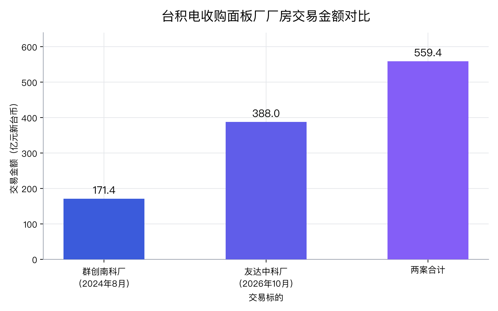
The two transactions were separated by over two years. On August 15, 2024, TSMC announced the acquisition of the Innolux South Technology Plant and its ancillary facilities for NT $17.14 billion; On October 29, 2026, it will take over the AU Optronics plant for NT $38.8 billion, with a total investment of NT $55.94 billion. For AU, the disposal benefit of NT $18.5 billion is a significant cash recovery in terms of finance, but the disposal benefit can only be recognized after the completion of delivery and other conditions are met, and it is expected to be difficult to account for within the year. It is worth noting that on the same day, AU Optronics announced that the transaction of selling Guangda's Huaya factory for NT $19.7 billion had been terminated due to the lack of consensus between the two parties on the specifications and delivery schedule of the factory, and the estimated disposal benefits of approximately NT $13.39 billion could not be realized as originally planned. TSMC Chairman Wei Zhe jia gave an answer outside of buying a factory at the press conference: the company has already mass-produced 5x mask size packaging, continued to promote 9x and 14x, and developed CoPoS; At present, CoWoS is still the preferred choice for customers, and the company will continue to provide sufficient production capacity.
Circular wafers cannot accommodate AI chips, packaging turns circles into squares
Why can panel factories enter semiconductor packaging? The answer is hidden in geometry. Square or rectangular packaging is configured on a 300mm circular wafer, leaving space at the edges that cannot accommodate a complete package; The larger the chip size, the more obvious the layout restrictions, and the number of complete units that can be produced per wafer decreases, making it more difficult to allocate costs. This has prompted manufacturers to seek panel level packaging solutions. According to a research report by Huatai Securities, the packaging area of NVIDIA Rubin GPU has reached 5.5 times that of the photomask, and a 12 inch circular wafer can only package 7 or even 4 chips.
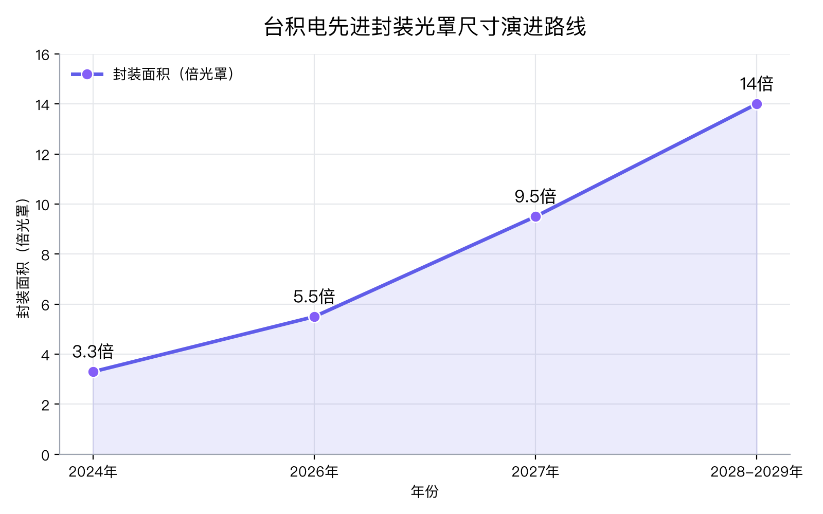
The pressure on the demand side is equally urgent. According to J.P. Morgan's report, TSMC's CoWoS production capacity is expected to reach approximately 33000 pieces per month by the end of 2024, 95000 pieces per month by the end of 2026, and 112000 pieces per month by the end of 2027. The compound annual growth rate of production capacity from 2022 to 2026 exceeds 50%, but the order fulfillment rate is still only about 80% by the end of 2026. The advanced packaging roadmap disclosed by TSMC at the San Jose Forum in April shows that the packaging area will increase from 3.3 times the mask size in 2024, 5.5 times in 2026, and 9.5 times in 2027 to 14 times in 2028-2029.
CoPoS (Chip on Panel on Substrate) is the solution that carries this transition: shifting some packaging processes from circular wafers to square panels, improving layout flexibility, and supporting the integration of large AI chips and multiple grains. Taking a 510 × 515mm panel as an example, the space available for placement is 4.5 times that of a 12 inch wafer; The chip output of a 600 × 600mm panel can reach 5 to 6 times that of traditional wafers. TSMC has standardized various panel sizes: 310 × 310mm is the main trial production, 510 × 515mm is planned to enter pre production simulation in the second half of 2027, and the ultimate goal is to advance to 750 × 620mm.
The glass core substrate belongs to the carrier material layout, which improves warpage and transmission problems through high flatness, dimensional stability, and low signal loss. Supply chain validation data shows that after importing glass substrates, packaging warpage related indicators improved by 16%, effective thermal expansion coefficient decreased by 19%, resistance value decreased by 27%, and inductance value decreased by 42%. Compared with CoWoS, CoPoS involves glass substrates, large-sized rewiring layers, low warpage control, and a new measurement and detection system. The number of RDL layers in panel level packaging is being upgraded from 3 to 9, and the distance between routing and bumps has been reduced from 20 microns to 5 microns. The industry has set its technical goal for the next 5 years at 2 microns.
In terms of mass production pace, TSMC's first CoPoS test line has been launched at the Caiyu Longtan plant, and will be relocated to the AP7 plant in Chiayi. Initially, it will be cut in with a panel size of 310mm × 310mm, and equipment and material verification will be carried out in 2026, followed by small-scale trial production in 2027. The market is expected to move towards mass production from the second half of 2028 to 2029. The first batch of equipment supply list has also been exposed. In addition to long-term partners such as Canon, Germany's SUSS, Japan's TEL, SCREEN, Applied Materials, and Koley, new manufacturers such as Panlin Group, Beilike, and Xinyun have jointly invested in key processes such as copper plating, exposure, surface mounting, mold sealing, and testing. However, differences still exist: substrate giant Feidian has evaluated that TGV technology will not be able to meet commercial mass production conditions until around 2030; Industry insiders have also revealed that the mass production of TSMC CoPoS has been postponed from the previous plan to 2028; Wei Zhejia bluntly stated that the scaling up of CoPoS production capacity still requires 2 to 3 years of development time.
The two tigers of the panel go their separate ways, heading towards advanced packaging together
In the long-term environment of oversupply in the panel industry, the consolidation of the dual tiger panel factory area and the release of high specification clean rooms have become targets for semiconductor factory expansion; Selling factories brings substantial profits, and the combination of factory sales and technological cooperation allows panel factories to gain entry into the semiconductor industry. For AU and Innolux, these are two paths under the same era proposition.
AU is using a combination of asset activation and glass substrate. In the past year, AU Optronics has successively disposed of its Kaohsiung Lujhu Color Filter Factory (sold to Sunlight for NT $6.3 billion, with a disposal benefit of approximately NT $4.28 billion) and its Singapore factory (sold to Western Digital for NT $350 million). Among them, the disposal of factories in Kaohsiung and Singapore had already accumulated a total of NT $34.7 billion. After the Zhongke plant transaction, AU Optronics Chairman Peng Shuanglang clearly stated that "asset revitalization will come to an end", and the recovered funds will be fully directed towards strategic and future investments; There are also market reports that the old factory of AUO Longtan is actively seeking buyers.
From a financial perspective, selling factories is about stopping bleeding rather than generating blood. AUO's consolidated revenue for the third quarter of 2026 was NT $66.88 billion, a quarterly decrease of 5.7% and an annual decrease of 4.3%. The net operating loss was NT $2.37 billion, with a net loss attributable to the parent company of NT $2.5 billion; The proportion of non display business revenue in the first quarter of 2026 has reached about 50%. Industry insiders bluntly state that the disposal of NT $18.5 billion in benefits addresses the balance sheet and cash flow issues, but does not solve the profitability problem of the panel industry.
From a technical perspective, AU Optronics has established an Innovation Research Institute to integrate its accumulated glass process and optoelectronic technologies over the past 30 years, plan TGV, RDL, and glass core substrate trial production lines, and combine Corning glass materials to support 510 × 515 mm glass substrates on the platform; Corning is responsible for glass modification and drilling, while AU carries out electroplating and circuit production. The division of labor and customer combinations for mass production have not yet been finalized. The company's board of directors has approved a new capital expenditure budget of NT $5.728 billion for the optimization of production lines and the layout of new technologies in the innovation research institute. In terms of transformation direction, Peng Shuanglang has given a clear timetable: by 2030, the proportion of direct sales of traditional panels will be reduced to 30%, and the remaining 70% of revenue will be driven by extended new business platforms; In the field of advanced packaging, AU is mainly positioned as a supplier of key components for glass substrate processing, and it is expected that the maturity and small-scale promotion of new technologies will take about 2 to 3 years. AU Optronics has previously entered the semiconductor supply chain through AU Optronics and Yupei, and the total revenue of related businesses exceeded $100 million last year. It is expected to maintain double-digit growth this year. Optical communication is another main line: AU has developed the optical engine required for optical interconnection rather than a complete CPO package. The plan combines Fuchai's Micro LED and VCSEL light source technology, Dingyuan's receiving components, and its own glass process capabilities to reduce energy consumption to 5% to 10% of existing solutions in specific applications; There are also reports in the industry that Intel is expanding its advanced packaging track for Micro LED substrates and is interested in collaborating with AU to develop CPO and high-density computing chip integration solutions.
Mass innovation will first land with FOPLP (Fan out Panel Level Packaging), and then move deeper into glass substrates. As early as 2017, Innolux has been investing in panel level fanout packaging, using panel production lines for IC packaging, and developing high-end semiconductor packaging with thin line widths using 3.5-generation line FOPLP glass substrates. In August 2024, Innolux sold its South Tech factory to TSMC for NT $17.14 billion, which was interpreted as a "factory plus cooperation" entry ticket for semiconductor panel factories in the market. Since the start of shipments in 2025, the monthly production capacity of Innolux FOPLP has rapidly increased from 4 million pieces to over 40 million pieces, and orders from its only US customer are expected to continue until the fourth quarter of 2026; The company is also promoting customer certification for RDL First and TGV technologies. The industry generally believes that these two technologies have more strategic value for its long-term layout of panel level packaging compared to the shipment volume of Chip First processes.
In September 2026, Innolux released its Chip List post chip packaging technology platform for the first time, with plans to enter mass production in the second half of 2027. The platform uses the industry's largest 620mm × 670mm panel substrate, which can achieve a minimum line width of 2 microns and a line spacing of 2 microns for processing; For the early implementation of the Chip First process, Innolux has developed a panel level testing system that can simultaneously test up to 64 chips, increasing testing efficiency by 50% to 80%. The original TFT display factory has been transformed and upgraded to an advanced packaging production line, creating a one-stop service chain for bare chip testing, chip packaging, and finished product inspection. The binding with TSMC is even more direct: TSMC announced in June 2026 that it would collaborate with Japanese companies such as Infineon and Innolux to develop glass core substrates, and with Corning to develop special glass vehicles; Innolux utilizes its Tainan factory to handle critical TGV processes. According to supply chain sources, Nvidia is testing glass core carrier boards and planning to have Innolux responsible for the front-end TGV. The industry believes that the inclusion of crowdsourcing in TSMC's cooperation list is a sign of panel manufacturers entering TSMC's packaging ecosystem.
Glass substrate competition: giants surround, re evaluating the value of old production capacity
TSMC is not alone. Intel was one of the earliest companies to lay out glass substrates. In January 2026, it announced that glass substrate technology had entered the mass production stage. The first Xeon 6+"Clearwater Forest" server processor equipped with a glass core substrate was unveiled at CES, and a giant glass core substrate prototype with integrated EMIB technology and a size of 78mm × 78mm was publicly displayed. Apple has started testing glass substrate samples supplied by Samsung Motors for its AI server chip codenamed "Baltra"; Broadcom and TOPPAN collaborate to develop glass core carrier boards, targeting the next generation of Tomahawk switch chips with a 510 × 510 mm specification; Samsung integrates Samsung motors and Samsung display resources to synchronize layout, with a panel size of 415mm × 510mm, and guarantees the source supply of glass core materials through a joint venture with Sumitomo Chemical in Japan; Rapidus uses 600mm × 600mm rectangular glass panels and plans to mass produce them by 2028; SKC's Absoluts glass substrate factory in the United States has provided production grade samples to customers and entered the certification stage, while LG Innotek focuses on CPO related technology.
The Chinese Mainland camp is also accelerating. BOE has a full process of glass substrate loading plate, 20 layers of large-sized glass substrate loading plate samples have passed six semiconductor level reliability tests, and samples are sent to the head AI chip manufacturer in Chinese Mainland. Chen Yanshun, chairman of the board, said he is preparing to invest in the semiconductor glass substrate loading plate mass production line; Woge Optoelectronics has built its first TGV production line with an annual output of 100000 square meters and achieved small-scale supply; There are also reports that Huawei is collaborating with BOE and Visionox to promote the mass production of semiconductor glass substrates. From the perspective of industry pace, 2026-2027 is a critical window period for glass substrates to transition from technical validation to small-scale mass production.
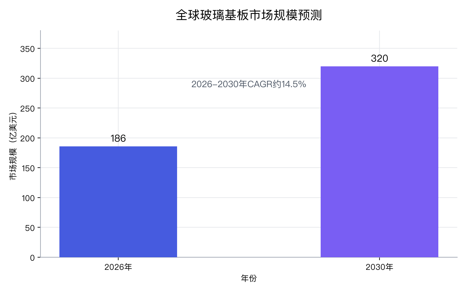
The market space is opening up. According to Omdia research, the global glass substrate market is expected to reach $18.6 billion by 2026 and is expected to exceed $32 billion by 2030, with a compound annual growth rate of 14.5% from 2026 to 2030; The market size of semiconductor TGV glass substrates is expected to reach 4.8 billion US dollars in 2026, a year-on-year increase of 50%.
However, there are still tough battles to be fought from the laboratory to the production line. The current mainstream solution for TGV pore formation is picosecond/femtosecond ultrafast laser modification combined with wet etching. Microcracks generated during laser drilling, copper plating, or heat treatment may extend to adjacent TGVs, affecting electrical performance and packaging yield. Therefore, detection is considered a key step in CoPoS mass production; The focus of industry competition is also shifting from substrate processing and TGV drilling technology to the iteration of polymer dielectric materials suitable for high-level RDL stacking. The panel factory also needs to gain the trust of semiconductor customers and prove its ability to provide stable supply of glass substrate materials. In addition, there is no unified standard for the size of each panel, and multiple specifications such as TSMC 310mm × 310mm, Samsung 415mm × 510mm, and Rapidus 600mm × 600mm coexist, which poses a challenge to the technical compatibility of equipment and material suppliers.
The same factory building is an inefficient old production capacity under panel logic, but a scarce physical entrance under semiconductor packaging logic. Market observation points out that the speed at which AI computing power devours advanced packaging has exceeded TSMC's ability to move within the existing wafer fab system. The cleanroom level, factory facilities, and large-span space of the panel factory, after renovation, perfectly match the requirements of panel level packaging for "large size, low vibration, and high cleanliness"; Part of the old production capacity of panels with location, clean room specifications, and space renovation conditions is transitioning from factory closure and production reduction to cross industry reassessment of asset use. For AU and Innolux, the funds from selling factories are used to invest in new technology research and development, while the ability to process large-sized glass is sought to be re integrated into the AI supply chain in the form of TGV, RDL, and glass core substrates. It remains to be seen whether AU can connect with TSMC's CoPoS requirements through asset activation, trial production, or technical cooperation in the future; It can be confirmed that the disposal benefit of NT $18.5 billion is not only financial income, but also a directional document.
