


Samsung customizes HBM4E for Meta, using a 2nm process for the logic substrate
On November 13, 2026, Korean media outlet The Bell cited industry sources reporting that Samsung Electronics is developing customized high-bandwidth memory (HBM) for Meta's self-developed AI chips. The product is based on the seventh-generation HBM4E, and the logic substrate (base die) will be manufactured using Samsung's own foundry 2nm process. If it ultimately launches, Meta will become the next giant after NVIDIA and AMD to secure Samsung's "exclusive" HBM.
(Headline of The Bell report)
On-demand customized HBM
To understand the weight of "custom HBM," we first need to look at what changes have occurred in the logic substrate itself. HBM stacks multilayer DRAM vertically, with the bottom substrate responsible for transferring data between the storage stack and the processor. In the HBM3 and HBM3E eras, substrates were manufactured by memory manufacturers using their own DRAM processes, and the number of logic circuits that could be implemented was quite limited. Starting with HBM4, substrates officially switched to logic process manufacturing, allowing customers to customize their layouts.
Samsung announced in February 2026 the shipment of the world's first commercial HBM4 products, with single-stack bandwidth up to 3.3TB/s, 2.7 times higher than HBM3E. According to Samsung Semiconductor's official website, HBM4 is built on sixth-generation 1c DRAM and 4nm foundry technology. Starting with HBM4E, Samsung's HBM product line was officially split into two lines: the standard version and the custom version. The standard version continued to use the 4nm substrate, while the custom version was developed according to the customer-specified process.
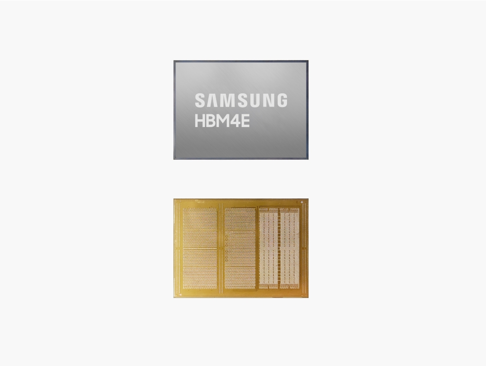
What is inside the substrate Samsung customizes for Meta? The report revealed that the initial customized logic substrates will integrate an HBM controller with die-to-die (D2D) interface IP, reducing data transmission power consumption by optimizing the storage interface. This aligns with the industry's technical direction of "sinking" controllers onto substrates—except Nvidia is deploying its own controllers, while Meta asks Samsung to design according to its chip needs.
Samsung custom HBM customers
Before Meta, NVIDIA was the initiator of this wave of customized HBM. In August 2026, NVIDIA will release its own custom HBM specification, NVHBM, moving the storage controller originally located on the GPU onto the HBM substrate. According to NVIDIA's official specifications, NVHBM offers up to 30% bandwidth increase and 15% lower power consumption compared to standard HBM4E, while freeing up up to 25% of the computing chip's area. To achieve cross-supplier consistency, NVIDIA requires all NVHBM substrates from Samsung, SK Hynix, and Micron to be manufactured using TSMC's 3nm process, with the memory cores uniformly using the sixth-generation 1c DRAM process.
AMD is taking a different path—tied to Samsung's own production capacity. According to South Korea's Daily Business Newspaper, Samsung plans to use Taylor's second factory in Texas (Taylor Fab 2) to produce 2nm HBM substrates for AMD and Nvidia, with AMD accounting for most of the reserved capacity. What is currently confirmed is that Samsung clearly stated in its Q3 financial report on October 29 that its foundry business revenue benefited from "HBM substrate sales growth."
Meta is a new customer in this landscape. SK Hynix also confirmed during its Q3 earnings call that it is collaborating with major customers to develop customized HBMs for their systems and workloads, with HBM4E samples shipped in Q2. In other words, custom HBM is no longer the exclusive domain of any one customer, but a standard service for leading storage manufacturers.
Meta's MTIA chip
Samsung is willing to invest in custom 2nm production capacity for Meta because Meta's self-developed chips are no longer just for show. Meta's MTIA (Meta Training and Inference Accelerator) began with the first generation released in May 2023, using TSMC's 7nm process, with a TDP of only 25W, focusing on recommendation system inference. The second generation, released in April 2024, shifted to TSMC's 5nm process, boosting overall performance to three times that of the previous generation at 90W power consumption, and has been deployed in 16 data center regions.
The real turning point will be on March 11, 2026. Meta officially announced four generations of chips: MTIA 300, 400, 450, and 500: MTIA 300 is already in mass production, used for sequencing and recommendation model training, with FP8 computing power of 1.2 PFLOPS and 216GB HBM. MTIA 400 offers a fivefold increase in computing power, supports 72-chip expansion domains, has completed lab testing, and is currently being deployed. MTIA 450 doubles HBM bandwidth from 9.2TB/s to 18.4TB/s, with mass production planned for early 2027. The flagship MTIA 500 will further increase HBM bandwidth to 27.6TB/s, with a maximum capacity of 512GB, and mass production planned for 2027.
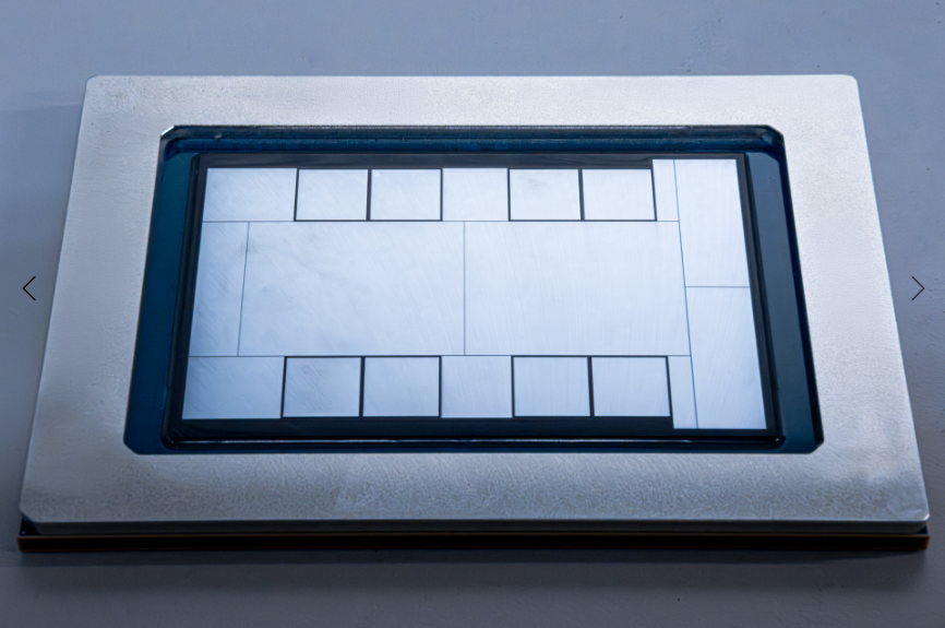
(MTIA chip rendering)
Between the four generations, HBM bandwidth increased by 4.5 times, computing power by about 25 times, and the iteration cycle was compressed to about every six months. The chip is jointly developed by Meta and Broadcom, with TSMC handling the foundry. Meta's Vice President of Engineering, YJ Song, explained this approach in an interview with Wired: "Instead of betting once and waiting for a long cycle, we consciously take an iterative approach, with each generation of MTIA building on the previous generation and using modular chipsets." "
Meta did not fully bet on self-development: in February 2026, Meta and AMD reached a long-term AI infrastructure partnership. Previously, it had also signed large purchase agreements with NVIDIA and AMD. The combination of "custom HBM + purchased GPUs," combined with a six-month chip iteration schedule, is Meta's most distinctive approach from other self-developed chip manufacturers.
