


The first 'Flying Sky', where exactly has domestic semiconductor equipment reached?
In 2026, the term that the Chinese semiconductor equipment industry lacks the least is 'first machine'.
From the beginning of the year to the end, domestic semiconductor equipment manufacturers have announced a 'first domestic machine' almost every few days. Series high-energy hydrogen ion implanters, critical dimension measuring CDSEMs, advanced gas cluster ion beam etchers, EUV light source prototypes—various 'national firsts' and 'global premieres' are dazzling. So we can't help but ask, after so many equipment challenges have been overcome, where exactly does the domestic equipment manufacturing chain stand as a whole? Which segments are already competitive, which are still tough nuts to crack, how does it differ from foreign giants, and where is it stronger?
Why are there suddenly so many 'first domestic units' this year?
This year, the highlights of domestic equipment came one after another. In January, the first series-type high-energy hydrogen ion implanter POWER-750H developed by the China Institute of Atomic Energy of the China National Nuclear Corporation successfully produced its beam. According to official statements, its core indicators reached international advanced levels, filling a long-missing link in the power semiconductor manufacturing chain. In June, the first critical dimension measurement equipment CDSEM independently developed by the 48th Research Institute of China Electronics Technology Group completed whole-machine debugging and factory inspection and was delivered to customers. This measurement equipment, known as the 'nanometer ruler,' had previously been almost entirely monopolized by overseas manufacturers. Around the same period, North Huachuang released the 12-inch advanced gas cluster ion beam etching equipment AcmeGlaion130 and launched the third-generation 12-inch all-quartz vertical silicon nitride LPCVD equipment. At the exhibition in October, Langdao Suiyan showcased the most advanced domestic EUV light source prototype in terms of public progress, claiming that the overall localization rate had reached 90%.
AMEC has truly pressed the fast-forward button. In March, it launched four new products, and in September, another six, covering areas such as extremely high aspect ratio etching, PECVD, ALD molybdenum metal deposition, and silicon carbide epitaxy, achieving high-density product releases twice within six months. By 2026, AMEC is expected to have accumulated over 8,800 reaction stations across more than 220 production lines domestically and internationally.
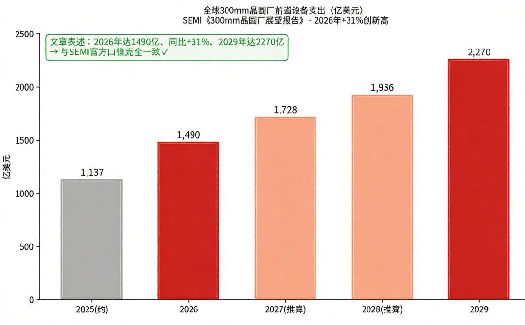
Behind this is the overall market boom. The '300mm Fab Outlook Report' released by SEMI at SEMICON West shows that global front-end 300mm wafer fab equipment spending is expected to reach $149 billion in 2026, up 31% from about $113 billion in 2025, setting a historic high; in the following years, this investment will continue to grow at a double-digit rate, reaching $227 billion by 2029.
The frequent appearance of the first units indicates that the technical bottlenecks of domestic equipment are being gradually overcome. Ten years ago, the industry was anxious about whether it could produce etching machines and cleaning machines; today, the topic has shifted to whether the entire industry chain of equipment can be completed, which represents a qualitative change at the ecological level. But we should view the 'first units' calmly: there are several hurdles between a prototype and mass production, from mass production to stable large-scale delivery, and then to being used as the main machines by leading wafer fabs.
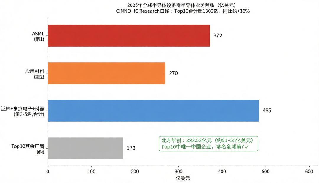
In the 2025 global rankings of equipment manufacturers, ASML topped the list with approximately $37.2 billion in semiconductor business revenue, Applied Materials was second with about $27 billion, and Lam Research was third with $23.2 billion for fiscal year 2026. Tokyo Electron and KLA ranked fourth and fifth, respectively. The top five collectively account for nearly 70% of the global market. North Huachuang is the only Chinese company in the global top ten, with 2025 revenue of 39.353 billion yuan, approximately $5.5 billion.
In the segments that can already be competitive, where are the domestic advantages?
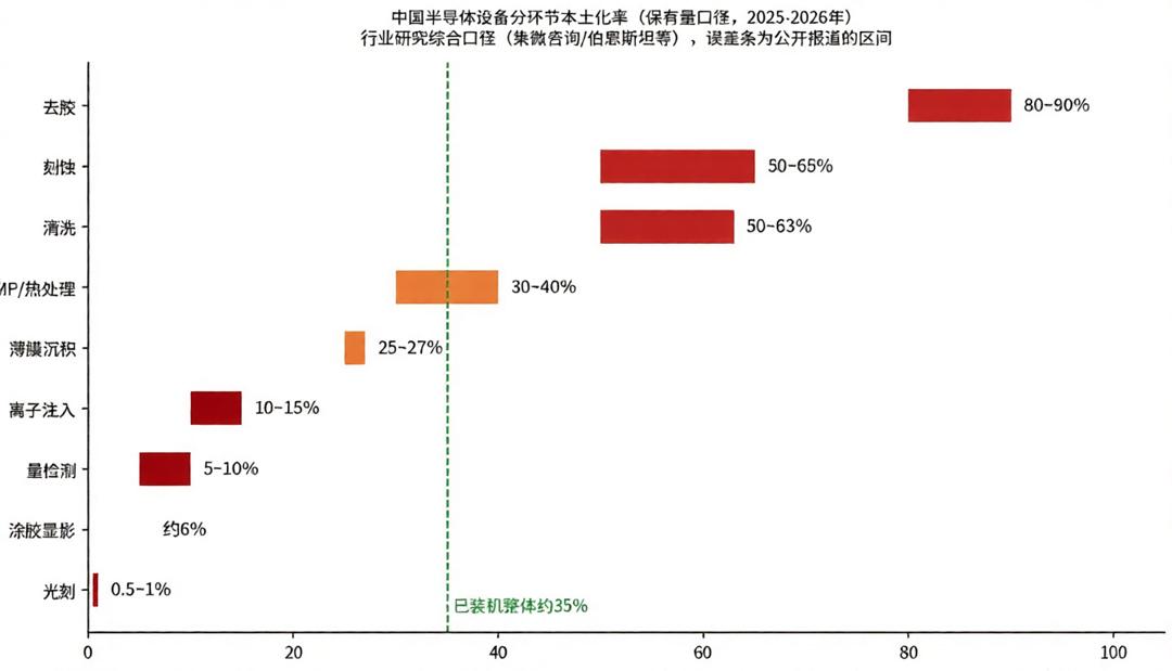
If the equipment is stratified according to localization rate, the top layer consists of degluing equipment. For mature processes of 28nm and above, the localization rate is about 80% to 90%, making it the most self-sufficient link in the entire process chain. Yitang Semiconductor, with the world's second-largest market share (about 33.7%), has become the main beneficiary of this segment. Domestic production lines have basically freed degluing equipment from external dependence. Further down are the major processes of etching, cleaning, CMP, and thermal treatment, which have already established large-scale deployment in mature processes.
Cleaning equipment was one of the earliest breakthroughs for domestic devices. Shengmei Shanghai started with differentiated innovation, with its product line covering approximately 95% of cleaning process steps. According to Gartner, its global market share of cleaning equipment is about 8.3%, ranking fourth worldwide and accounting for 60.5% of the domestic market for local cleaning equipment, with the overall domestic share second only to Japan's DNS. Shengmei has also entered the electroplating and advanced packaging equipment sectors and has delivered single-wafer cleaning equipment to overseas customers in Singapore and other countries, marking a symbolic step for domestic equipment moving from internal competition to overseas expansion.
CMP equipment serves as a 'model room.' Huahai Qingke almost monopolizes the domestic CMP market, accounting for more than 90% of local CMP equipment sales, and its share in procurement by some leading domestic integrated circuit manufacturers can reach over 90%. Advanced process models have already passed full-process verification at multiple leading wafer fabs. Its path is very representative: it first excels in a single segment and then expands outward. Nowadays, Huahai Qingke is also planning for ion implantation equipment.
Etching and thin-film deposition are the two segments with the largest market size and the highest technological content, and local manufacturers have achieved the most solid breakthroughs here. Zhongwei's CCP etching equipment has long been used in TSMC's 5nm production line, serving as a card of honor that local equipment can enter the world's most advanced production lines. North Huachuang's etching and thin-film deposition equipment revenue will both exceed 10 billion yuan in 2025, covering mature processes of 28nm and above, and extending to more advanced nodes. Tuojing Technology has been deeply cultivating the field of thin-film deposition and expanding into advanced packaging and hybrid bonding. Etching and thin-film deposition share core technological bases such as plasma physics, vacuum chambers, and RF power; the experience an enterprise accumulates in etching can be reused in deposition equipment. This is why local manufacturers can quickly build platforms in these two segments.
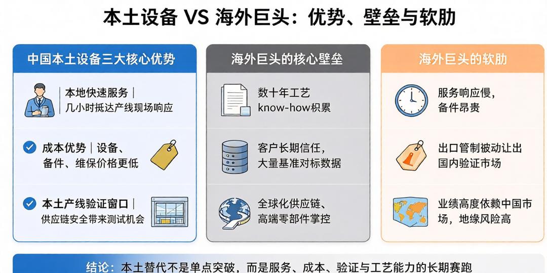
The core advantages of domestic equipment can be summed up in three points. First is local service: when a wafer fab encounters a problem, domestic manufacturers can arrive on-site within hours, providing a level of responsive support that overseas giants cannot match. Second is cost: for the same performance, domestic equipment is usually significantly cheaper, and spare parts and maintenance are also inexpensive. Third is the customer validation window: due to supply chain security considerations, domestic wafer fabs are more willing than ever to open their production lines to validate domestic equipment. This 'opportunity to be trusted' has been the rarest resource in the past decade. Zhongke Feice has cumulatively delivered about 2,000 metrology devices.
Middle zone, climbing but still struggling
Beyond large markets such as etching and cleaning, there is a 'deep water zone' with high technical difficulty and a relatively small market size, where the localization rate is still in the single digits to just over ten percent. Ion implantation, metrology, and coating & developing are the most typical representatives.
Ion implanters are known as one of the 'four core equipment' in chip manufacturing, but the overall domestic localization rate is only about 15%, with large-beam models accounting for less than 10%. The most critical issue is that the world's most advanced ion implanters are banned from export to China, and even corresponding second-hand equipment cannot be procured. Domestic wafer fabs can only use outdated models, directly affecting yield and stability. Players in this field are increasing; Zhongkexin and Kaishitong are familiar names, while Aien Semiconductor, Sirui Intelligent, Jing Sheng Electromechanical, and North Huachuang have also entered the market. Aien has already formed a full-spectrum matrix covering medium-beam, large-beam, high-energy, and special ion implantation. Sirui Intelligent's high-energy and large-beam models have been shipped, and Jing Sheng Electromechanical's silicon medium-beam models are under customer verification. However, almost all players have not yet turned a profit and are generally in the stage of high R&D investment. The difficulty of ion implantation lies in the non-transferable technical path. Its core is ion optics, electromagnetic mass analysis, and high-voltage acceleration, making it more like a particle accelerator rather than conventional process equipment; experience with etchers cannot be easily transferred. The first serial high-energy hydrogen ion implanter beam-out is good news, but the road from beam-out to being able to reliably support mass production of advanced power devices is still long.
Metrology equipment is one of the segments with the lowest localization rate, less than 10% in previous years. Wafer fabs have a very high trust threshold for it because metrology does not directly manufacture chips but determines whether a wafer is qualified or scrap; even the smallest defect can cause the entire batch to be discarded. However, the progress over the past two years has been visible to the naked eye. Zhongke Feice's equipment types that have been mass-produced and verified account for over 70% of the total quality control equipment market. Bright and dark field defect inspection has achieved a high replacement rate in the four major wafer fabs. Yuwei Semiconductor's mask inspection equipment has reached top overseas levels and can fully replace them, and Dongfang Jingyuan's CDSEM measurement repeatability has achieved 0.15 nanometers. China Electronics Technology Group Corporation's 48th Research Institute has also delivered its first CDSEM to customers. Nevertheless, industry insiders admit that leading wafer fabs still retain imported equipment as a benchmark when making new purchases. Domestic equipment must match and compare testing results with overseas machines to verify performance. This trust barrier has not yet been completely dismantled.
The localization rate of coating and developing equipment is about 6%. This sector has long been monopolized by Tokyo Electron and DNS. Chinyuan Micro and Shengmei are entering head storage customer verification. Once breakthroughs occur, the replacement potential is huge, but it is still in the introduction stage.
The toughest bones are still lithography and bonding.
If we say that deep water areas are difficult, then lithography machines and hybrid bonding are 'the most difficult of difficulties,' areas that domestic equipment truly cannot reach.
Lithography is the largest single category in semiconductor equipment and also has the lowest localization rate domestically, less than 1%, almost entirely dependent on ASML, Nikon, and Canon. Shanghai Microelectronics is the only major domestic player; the exhibited I-line scanning projection lithography machine has a resolution of 280 nanometers, and the KrF dry lithography machine has a resolution of 110 nanometers, with a cumulative customer production exceeding 10 million wafers. The EUV lithography machine upstream is an unavoidable ceiling. The EUV light source prototype from Longdao Suiyan claims a 90% localization rate, but the remaining 10% often consists of the most critical components, which could be special optical materials, ultra-high precision sensors, or laser components of specific specifications. The logic of semiconductor equipment is that if any single component is unavailable, the entire machine becomes scrap metal. The head of Zeiss's semiconductor division publicly stated that China is approximately 15 years behind the West in EUV technology. UBS analysts infer that China may be able to produce models that can replace ASML's top-tier equipment at the earliest in 10 years. Domestic EUV, from light source prototypes to commercial use, still has a long road of engineering development.
The D2W hybrid bonding equipment in advanced packaging is another tough nut to crack. In the post-Moore era, advanced packaging has become a key path for sustaining computing power growth, and bonding equipment directly determines chip performance and yield. Domestic companies like Qinghe Jingyuan, Tuojing, Xinhui Lianxin, and Xingkong Technology have all launched hybrid bonding products, but industry insiders speak frankly: the W2W process has long been mature, and the real challenge lies in D2W. Currently, D2W hybrid bonding equipment is mainly monopolized by the Dutch company BESI, and globally only TSMC has D2W process mass production capabilities. Domestic manufacturers are almost all at the verification stage and lack mature products for mass production. D2W is difficult in three aspects: downstream traction is lacking, as there are no domestic customers for D2W process mass production, making process parameter requirements unclear; verification resources are scarce, with limited high-value wafer materials from leading wafer fabs, making it hard for newcomers to gain production line verification opportunities; and cross-process collaboration has high barriers, since hybrid bonding needs to integrate front-end process capabilities like lithography compensation, making it a systems engineering challenge.
What are the strengths of foreign giants?
Foreign equipment giants can monopolize the high-end market thanks to decades of accumulation and first-mover advantages.
In the field of lithography, ASML has monopolized EUV lithography machines. By 2018, it had achieved a 250-watt light source power, and in April 2025, it completed a demonstration of a 1000-watt EUV light source, an engineering level that domestic prototypes cannot reach in the short term. ASML's dependence on the Chinese market is also deepening. In the third quarter of 2026, its sales to China surged 109% quarter-on-quarter, with China’s share jumping from 14% to 23%, contributing about 20% of annual revenue. Since 2023, mainland China has once been its largest global market, and in 2024 and 2025, its share exceeded 30%. This contrast is subtle: on one hand, sales to China are climbing steadily; on the other, high-end models are restricted, so what you always get is 'sufficient but not top-of-the-line.'
In the field of etching, Lam Research Group has a global market share of approximately 52.7%, with the top five global manufacturers accounting for 86.3% collectively. Lam Research also achieved an increase of about 210 basis points in market share by 2025, relying on the process advantages of high-end etching equipment. In the field of metrology, KLA holds a 46.2% market share in overlay error measurement in China, nearly half of the market. These giants still present barriers that local manufacturers find difficult to surpass in the short term, due to their process know-how in advanced manufacturing, years of accumulated customer trust, global service networks, and supply chains for core components.
But foreign giants also have their weaknesses. First is price and response: their equipment is expensive, spare parts are costly, service is slow, and localization is insufficient. Second is regulatory backlash: the more advanced the equipment, the more it is hindered by export controls, which ends up giving the Chinese market to domestic manufacturers. This is precisely the root of the window of opportunity for local equipment to gain validation. Third is the risk of 'over-reliance on a single market': if revenue from China accounts for too high a proportion, any changes in geopolitical policies could cause these giants' performance to fluctuate sharply.
Gaps, shortcomings, and a truthful statement
Putting the localization rates of each link together, the conclusion is very clear. Stripping, cleaning, and CMP are already close to or exceed half of self-sufficiency; etching, thin films, and thermal processing have established a foothold in mature processes; metrology, ion implantation, and photoresist coating/development are still being implemented and ramped up; lithography and EUV still rely almost entirely on imports. Overall, according to Korean media reports, the proportion of domestic equipment installed in Chinese wafer fabs has risen to about 35%, and in the first half of 2026, the revenue of eight equipment companies increased by 13.8% to 69%.
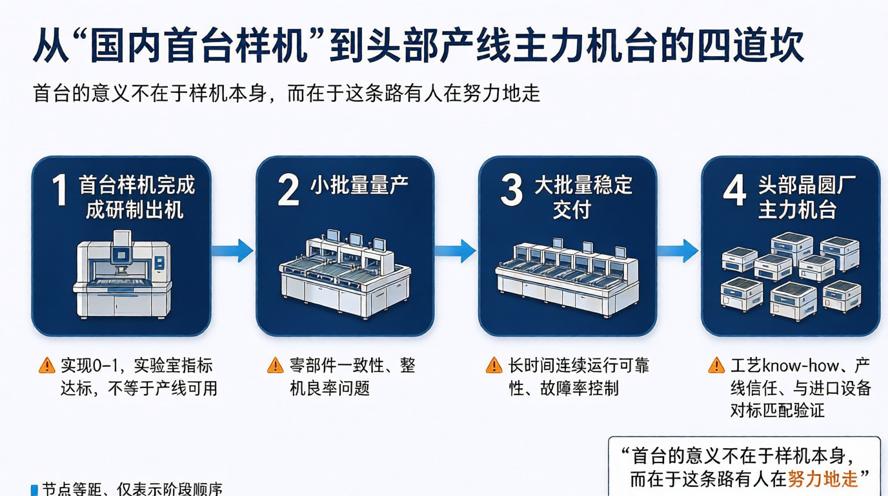
But the most critical bottleneck is in the manufacturing process. For devices of 28nm and above mature processes, the localization rate has already exceeded half, yet for 14nm and below advanced processes, the self-sufficiency rate in etching is less than 15%, and overall advanced processes are below 15%. Using equipment and processes from mature processes to bypass EUV for advanced processes requires continuous costs in yield and expense. At present, domestic equipment is not lacking in 'first units from 0 to 1'; what is lacking is the mass production stability of 'from 1 to N', process verification for advanced processes, and autonomy in core components. The 10% of imported components in EUV light sources is the most realistic reflection of this.
Another hidden concern is profitability. Ion implantation manufacturers are generally losing money, and most players in metrology and coating/developing are still relying on heavy R&D investment to persevere. Equipment localization is a long-term endeavor, not a sprint. The health of the industry is not only measured by whether the first machine has been produced, but also by whether these companies can survive on operating cash flow and continue investing in next-generation R&D. The easy part is already done; what remains is tough, and this statement reflects both the current situation and a reminder.
Objectively speaking, domestic semiconductor equipment has already reached a critical point. In terms of scale, China has become the world's largest equipment procurement market, providing domestic manufacturers with a verification and application ground that other countries do not have. Technologically, etching, cleaning, and CMP have already secured a place in the global industry chain, and platform-leading companies are beginning to emerge. The scale and product breadth of companies like SMIC Nanjing and North Huachuang already qualify them to compete with second-tier foreign manufacturers. Structurally, from process equipment to measurement and testing to packaging equipment and core components, players covering the full chain are emerging, and the ecosystem is taking shape.
The shortcomings are equally glaring: the gaps in lithography, the long-term challenges of EUV, the trust threshold in ion implantation and metrology, the mass production gap in D2W bonding, and the localization of core components. These cannot be solved by a single breakthrough; they require coordinated verification across the upstream and downstream of the industry chain and long-term, intensive investment. The advantage of foreign giants lies in decades of accumulated barriers, while the advantage of domestic equipment is close service, lower costs, and a local market willing to give it a chance.
Returning to the initial question, how far have domestic devices actually progressed? The answer is that they have succeeded in the mass market, are still struggling in the deep waters, and the toughest part, photolithography, still requires effort. The significance of the first machine does not lie in the prototype itself, but in the fact that it lets every link in the industry chain know that someone is on this path and has already passed the most difficult stage.
