


After TSMC, it's Samsung's turn: 8-inch ebb tide opens, mature process outsourcing brewing price increase
The industrial map of mature processes is being redrawn by AI. According to industry sources, Samsung Electronics has recently notified its 8-inch wafer foundry customers that it plans to completely cease related production line operations by the end of 2030 and focus its manpower and equipment investment on advanced processes for 12 inch wafers. This is the first time Samsung has provided a clear timetable for a comprehensive exit - in the past, the chip giant only stated that it would gradually reduce the size of its 8-inch production line.
1、 Timetable implementation: Countdown to the business with a monthly production capacity of 250000 pieces
Samsung's 8-inch outsourcing production capacity is concentrated in the South Korean Qixing Park, with three wafer fabs: S6, S7, and S8. According to the previous plan, the company had originally decided to close the S7 factory this year and maintain the operation of the other two. Kang Seok chae, Vice President of the Semiconductor Manufacturing Division, announced during the first quarter earnings conference call that 8-inch power semiconductor, display driver IC (DDI), and image sensor production lines will be gradually shut down; Starting from this year, Samsung wafer foundry will no longer undertake orders for new 8-inch products.
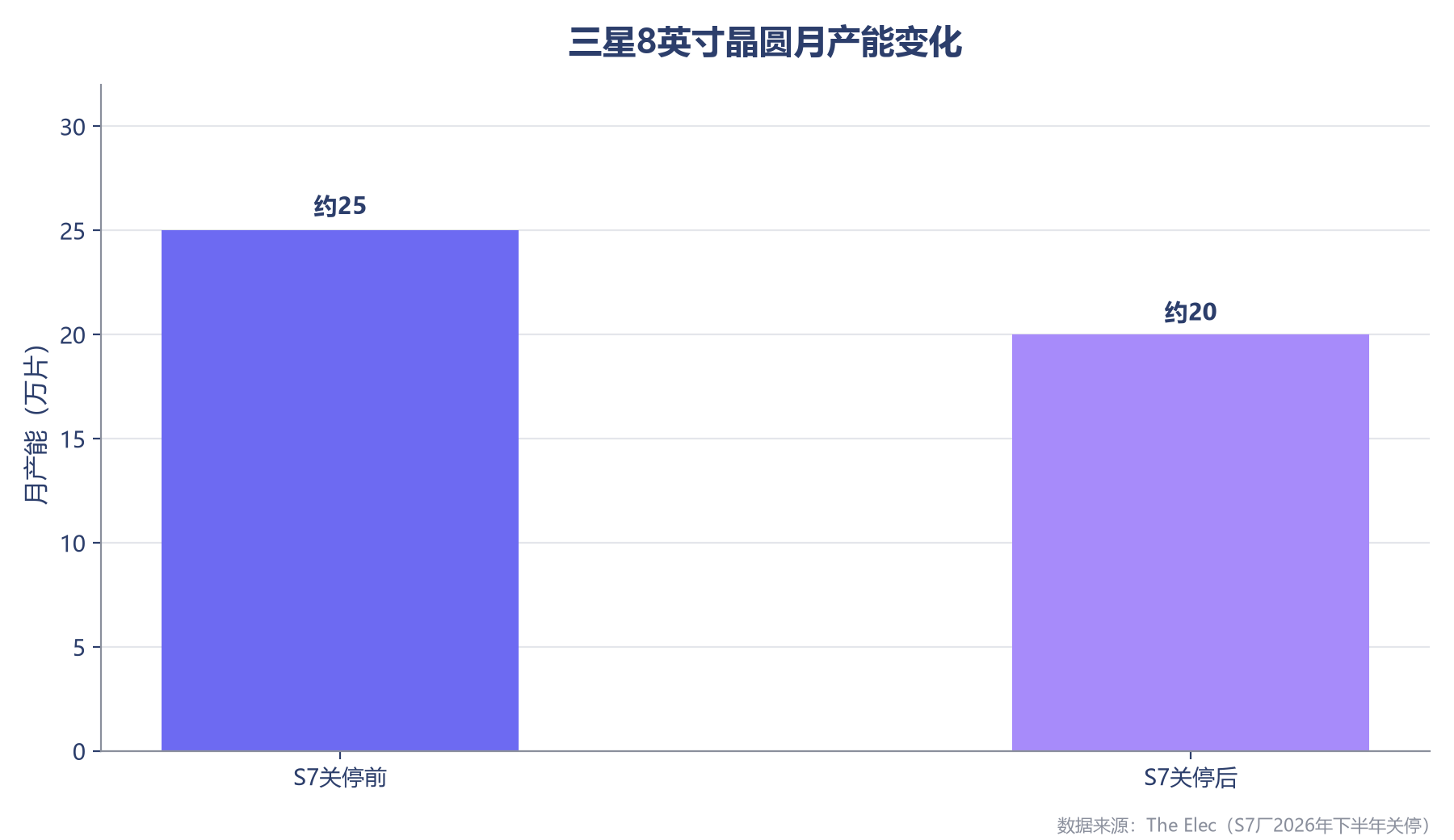
Shrinkage is being quantified and realized. According to reports, after the shutdown of S7, Samsung's monthly production capacity of 8-inch wafers will decrease from about 250000 pieces to below 200000 pieces, and the overall operating rate is currently only about 70%. Among them, S6 factory covers processes ranging from 0.13 microns to 0.35 microns, supporting BCD, power devices, and image sensors; The process range of S8 factory is between 0.18 microns and 0.5 microns, with a focus on photoelectric sensors and high-voltage analog circuits.
This production line carries a long development history - Samsung Electronics' 8-inch wafer foundry covers mature processes such as 65nm, 70nm, 90nm, 130nm, and 180nm, mainly producing various system semiconductors such as display driver ICs, power management ICs, microcontrollers (MCUs), and image sensors; Samsung launched mass production of the 180 nanometer process in 2000, and subsequently introduced 130 nanometer, 90 nanometer, and 70 nanometer processes in 2002, 2006, and 2011, respectively.
2、 Customer dilemma: Full load of local factories and nowhere to go orders
The most urgent thing is the Korean IC design company that has been entrusted to Samsung for long-term outsourcing. Customers such as ImageS, ABOV Semiconductor, Dongyun Anatech, Silicon Mitus, LX Semicon, etc. must transfer their existing products to other wafer foundries or ensure alternative processes before the shutdown deadline.
The problem is that there is not enough alternative production capacity. Representative companies DB HiTek and SK Key Foundry, which operate 8-inch wafer foundry in South Korea, have already occupied a large amount of production capacity by existing customers and are approaching full capacity, making it difficult to undertake orders transferred from Samsung; Some chip design companies have stated that if they want to add chips, they can only look for overseas foundries.
Turning to a 12 inch process is also not easy. The original customer's product has been designed based on a 90 to 180 nanometer process for a long time, and migrating to 12 inches may increase manufacturing costs and require redesign and product validation; Especially for simulating semiconductors that require special processes driven by high voltage, it is difficult to migrate by simply reducing the line width. Even if it turns to overseas, the situation is not optimistic: Taiwan, China's 8-inch production capacity is also not too much surplus, and the commissioning of Chinese Mainland enterprises may face the obstacles of the end customer's restrictions on the use of semiconductors made in Chinese Mainland.
Some chip design companies have prepared to seize the transition time by locking in Samsung's production capacity and accumulating inventory in advance, but the inventory strategy requires additional funds and warehousing costs, and will still need to be revalidated on alternative production lines in the long run. There are voices in the South Korean industry calling for Samsung to delay the closure schedule and urging the government to coordinate; However, some industry insiders have also expressed that Samsung has given manufacturers four years of preparation time, and this decision is difficult to say is a unilateral measure.
3、 Why Exit: Economic Accounts, Platform Migration, and AI Siphoning
The giant's retirement of 8 inches is not due to the disappearance of mature process requirements, but rather a combination of three considerations.
One is that the economic accounts are becoming increasingly unprofitable. The aging of 8-inch equipment, high maintenance costs, heavy depreciation pressure, and naturally limited profit margins; Under the same factory and labor costs, 12 inch wafers can produce more grains and are easier to achieve automation and scale. In the current era of explosive demand for advanced AI processes, Samsung's decision to "break away" is in line with business logic. The second is product platform migration - product lines with economies of scale such as CMOS image sensors and display drivers are accelerating their shift towards 12 inch platforms, and the product portfolio with 8-inch production capacity is becoming niche. The third is the "siphon effect" of AI: capital and engineering resources are flowing towards advanced processes and packaging with higher returns, and the priority of 8-inch resource allocation is naturally shifted backwards.
For Samsung, this is a crucial step in the strategic transformation of its foundry business: facing TSMC's leading advantage in advanced processes, Samsung is focusing on high value-added areas such as 12 inch GAA transistors, HBM supporting logic chips, and automotive grade MCUs, and improving business gross profit and capital return by divesting inefficient assets.
4、 8-inch ebb tide: a global capacity rearrangement
Samsung is not an isolated case. TSMC has gradually reduced its 8-inch production capacity since 2025. Its 8-inch Fab 5 is expected to cease operation by the end of 2027, and its 6-inch Fab 2 is also planned to close in the same year.
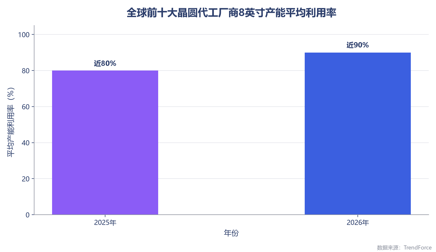
The mismatch between supply contraction and strong demand is reshaping the value of mature processes. According to TrendForce data, the total production capacity of 8-inch wafer fabs worldwide is expected to decrease by 2.4% year-on-year in 2026; Driven by the surge in demand for power management ICs, analog chips, and power devices from AI servers, the average utilization rate of 8-inch production capacity for the top ten global wafer foundries has rebounded to nearly 90% by 2026, a significant improvement from nearly 80% in 2025. Some foundry prices may increase by 5% to 20%. Another organization, Sigmaintell, has a more aggressive calculation: global 8-inch production capacity will be reduced by 6% this year and another 2% next year, with a capacity utilization rate of up to 91% at one point. Due to the difficulty of restarting the production line once it is retired, the 8-inch supply elasticity is approaching zero in the short term.
The production capacity gap has also begun to overflow and transfer orders. TrendForce pointed out that nearly 70% of the production expansion of the 12 inch mature process is driven by Chinese Mainland fabs, which are transferring DDIC and CIS production capacity to PMIC and power devices with better profits; Under the influence of Taiwan manufacturers' capacity transfer and price increase, the order transfer effect of HV manufacturing process and CIS customers turning to wafer fabs in Chinese Mainland began to appear in the second half of 2025, and the demand for wafer integration, which is dominated by low-end DDIC and CIS, has exceeded supply. In the medium to long term, the 8-inch product will not be phased out, but its positioning will shift to a manufacturing resource with higher costs and more focused applications. Mainstream mass production tasks will be taken over by mature 12 inch process platforms.
For Samsung, this is a full bet on AI computing outsourcing; For manufacturers who remain on the 8-inch table, the exit of giants has just brought a window of dividends - however, who can transform the current 8-inch dividend into the mass production capability of 12 inch characteristic processes, and who can seize the initiative in the next round of mature process competition.
