


Fast charging dividend exhausted, can gallium nitride keep up with the AI wave
A few years ago, gallium nitride entered the public eye through fast charging heads, relying on its high switching frequency and high power density characteristics to achieve a mass popularization of the power semiconductor field. Nowadays, the track pattern has been rewritten, and after the expansion of production capacity, price wars continue to compress profits, and the growth ceiling of the consumer market is visible to the naked eye. The industry is beginning to seek incremental growth, with car mounted OBC, 48V auxiliary power supply, and AI server HVDC power supply becoming key areas of focus for manufacturers.
Transitioning from consumer grade products to vehicle specifications and computing scenarios, the verification standards, failure risks, and delivery logic are all restructured. The wave of computing power is rolling forward, and the in vehicle verification cycle is long. Whether gallium nitride can catch up with this new demand and overcome the growth dilemma after the fast charging dividend fades, the answer is still in the long process of testing and targeted implementation.
Fast charging dividends peak, product line reaches a crossroads of differentiation
In recent years, gallium nitride has become a selling point for high-end fast charging, with 20W to 140W chargers being rolled out one after another, and mobile phone, laptop, and accessory manufacturers flocking in. From the earliest 65W GaN charger known as the charging revolution, to now being able to buy a fast charging head that supports multiple protocols for just a few tens of yuan, this market has completed the transition from a popular product to a standard product in just a few years.
According to industry research data, the domestic consumption of GaN fast charging shipments will exceed 220 million units in 2025, but the average unit price will drop by more than 60% from the high point in 2022, and the gross profit margin will fall from over 35% in the early stage to the range of 12% to 18%. The product forms are concentrated in 650V horizontal E-mode discrete tubes and simple half bridges. The design logic prioritizes controlling BOM costs, and the reliability verification cycle is short. Whoever can lower the cost of one tube will have an advantage in the overall quotation. When production capacity is released and solutions become increasingly homogeneous, price wars are inevitable, and the era of telling stories based on efficiency parameters is over.
The decline of the fast charging market dividend is directly reflected in the manufacturers' accounts. On the one hand, the unit price of gallium nitride devices continues to decline, while the volume increases but the profit margin narrows; On the other hand, whole machine manufacturers have increasingly strong bargaining power over components, forcing them to make more extreme trade-offs between cost, performance, and reliability. Manufacturers are forced to make product line trade-offs, with some continuing to delve deeper into the consumer market. The iterative direction is focused on optimizing Qg, miniaturizing packaging, and improving wafer yield, relying on cost advantages to increase volume and turn the fast charging market into a stock business that maintains cash flow; The other part will start building separate vehicle specifications and industrial product lines, redefining device specifications, establishing batch control rules, extending verification cycles, and exchanging time for higher gross margins and more stable orders. The target gross profit margin for automotive grade GaN devices is generally maintained at over 25%, which is about twice that of consumer grade products, but the investment in research and development and verification has also doubled.
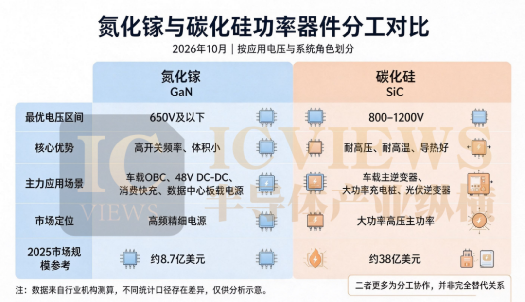
When discussing the application prospects of gallium nitride, one cannot ignore its relationship with silicon carbide, which are often confused. Many observers outside of the industry tend to view wide bandgap semiconductors as a whole, thinking that gallium nitride and silicon carbide are the same thing, and whoever has stronger performance will win. But their differences in application breadth and value stem from the division of voltage levels and switch characteristics, rather than who has stronger performance. In terms of market size, the global SiC power device market is expected to reach approximately 3.8 billion US dollars by 2025, while the GaN power device market is expected to reach approximately 870 million US dollars during the same period. The significant difference in size is due to the natural differences in scene division of labor.
The nature of silicon carbide lies in high voltage. It is a wide bandgap material with excellent pressure resistance, high temperature resistance, and thermal conductivity. Its main battlefield is in vehicle mounted main inverters, high-power charging piles, and photovoltaic inverters above 800V or even 1200V. These scenarios have high power and bus voltage, and silicon carbide can directly replace silicon IGBT, resulting in lower conduction loss and higher switching frequency. The value of a single device is also high, making it the most expensive and fastest-growing category of wide bandgap power devices. So a large number of reports on the third and a half generations are clustered on silicon carbide substrates and main drives in the market, because the story of silicon carbide is about high power, high value, and concentrated volume, which is the most direct to tell.
Gallium nitride is different, it excels in low voltage and high frequency. The current commercial GaN on Si lateral devices have a main voltage range of 100V to 650V, much lower than silicon carbide, but with extremely fast switching speed, high efficiency, and small size. Its home field includes 6.6kW to 11kW on-board OBC, 48V/12V DC-DC, industrial servo, communication power supply, and the increasingly popular onboard power supply for data centers. Silicon carbide is used for high-power and high-voltage coarse heavy work, while gallium nitride is used for high-frequency, high-efficiency, and compact fine work. The two are often divided and cooperate in the system, rather than replacing each other. This also explains why the gallium nitride market has always appeared smaller than silicon carbide, as its unit price, single scenario power output, and overall value are naturally lower than silicon carbide.
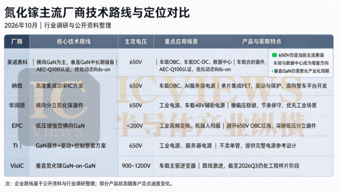
Similarly, in the field of gallium nitride, the product positioning of Innolux, Nano Micro, CR Micro, TI, EPC, and VisiC has clearly differentiated. Some are betting on production capacity and cost, some are betting on system level solutions, some are betting on integration, and some are simply bypassing the red ocean to target niche scenarios. This differentiation itself is a signal that the industry has entered the second half. Enterprises must balance the short-term revenue brought by fast charging with the long and high investment verification cycle of automotive product lines. This balancing technique precisely determines how far each company can go in the next few years.
Three technological leaps, each generation corresponding to different products
What truly determines the direction of this transformation is the evolution of gallium nitride device technology itself, and behind each round of evolution, there are different product solutions from various enterprises. Looking at the 20-year industry history, gallium nitride power devices have actually fought three tough battles, each corresponding to a generation of traceable products.
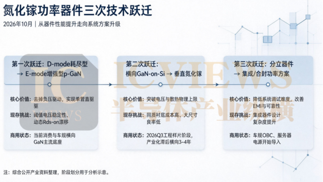
The first transition is from depletion type to enhancement type. Early D-mode depletion devices had to rely on negative voltage turn off for their gate, requiring an external cascaded silicon MOSFET to enter the system. The structure was complex and had many reliability risks. They were only tested in small batches in a few industrial scenarios, accounting for less than 5% of GaN power device shipments, and could not be considered for installation. After the p-GaN gate engineering made the device into an E-mode enhanced type, single tube direct drive without negative pressure circuit became the current commercial base.
But common pain points also follow, such as the stability of the threshold voltage Vth and whether the dynamic on resistance Rds on under high voltage dynamic stress will degrade, which determines whether this tube dares to be loaded onto the vehicle. Around this issue, each company has different actions. InnoTech iterated the third-generation Inno GaN p-GaN platform, optimized the buffer layer structure to suppress interface charge capture, and simultaneously submitted multi gate process samples to Tier1 for comparative testing; China Resources Microelectronics' automotive grade lateral gallium nitride devices focus on robust gate bias control solutions, initially targeting industrial power supplies and vehicle mounted 48V auxiliary power supplies, with a conservative rhythm; EPC is based on low-voltage enhanced devices and deliberately avoids the red ocean of 650VOBC, focusing on industrial high-frequency conversion and robot servo. The core of this first battle is who can make the gate more stable while maintaining high switching speed, and whose tubes dare to be truly installed into the system for long-term operation.
The second transition is from horizontal to vertical. Horizontal GaN on Si is currently the main production force, but at a voltage level of 650V, it is close to the ceiling of voltage resistance and thermal management. As the stack voltage and current increase, the cost of horizontal structure in terms of conduction resistance and heat dissipation path will sharply rise. The optimization of manufacturers focuses on buffer layer and epitaxial defect control to improve dynamic characteristics, but the physical limit of the lateral structure lies there. To achieve 900V or even 1200V, we have to bet on vertical gallium nitride, which is a GaN on GaN substrate with a structure where current flows vertically. As of the third quarter of 2026, vertical GaN is still in the stage of engineering sample delivery, with industrialization progress lagging behind horizontal GaN by at least 3 to 4 years. The cost of homogeneous substrates is 8 to 12 times higher than that of GaN on Si epitaxial wafers of the same specifications, with the focus on homogeneous substrate cost, dislocation density, and large-sized yield.
There is the greatest divergence in the strategies of various companies in this regard. VisiC chose to directly enter the vertical gallium nitride field, targeting the vehicle's main drive inverter, and jointly developing a prototype with AVL, which is a quite aggressive route; InnoTech is simultaneously laying out vertical gallium nitride research and development, but currently prioritizes resources on the landing of horizontal vehicle compliance products, treating the vertical route as a medium - to long-term technical reserve; At present, most domestic manufacturers still focus on horizontal platform iteration, and vertical gallium nitride is still at the level of laboratory wafer fabrication and academic cooperation, without a clear sample delivery plan. This second battle is about who can break through on the substrate and epitaxy first, and who can lift the ceiling of voltage levels even higher.
The third leap is from discrete devices to integrated solutions, which is also the track with the biggest divergence in current routes. Discrete devices have high flexibility and are suitable for Tier 1 with strong self-developed capabilities. The short board is loop parasitic and EMI debugging difficulty, which is mainly promoted by China Resources Microelectronics and EPC. The integrated solution packages GaN FET, gate clamp, Miller clamp, and short-circuit protection together, reducing the threshold for system development and becoming the mainstream direction for OBC implementation at present. The Solid Gallium Nitride Automotive Compliant Sealing Devices ISG6127ATPG-Q and ISG6129BTQ-Q, launched by InnoSeco, are 650V and integrated with Miller clamp, specifically designed to solve gate misguidance caused by high-frequency dv/dt. They have passed AEC-Q100 certification and are designed for 6.6kW OBC and vehicle DC-DC. Nano Micro's GaN Safe automotive grade power IC takes it to the extreme, integrating FET, driver, short circuit protection, and ESD protection on a single chip, with built-in GaN Sense detection, focusing on digital input and output power, and also supporting the development of OBC platforms for vehicle manufacturers. It even uses a 20-year limited warranty to dispel reliability concerns for car manufacturers. TI's approach is different. It does not solely focus on promoting gallium nitride devices, but relies on a complete power ecosystem to package gallium nitride power transistors and self-developed driver and control chips into reference designs for delivery, reducing the difficulty of traditional Tier1 porting. This third battle is essentially a battle of business models, where selling a tube and selling a power solution have completely different requirements for customer capabilities, and also determine the customer structure and bargaining power of each company.
There is a dark line running through the three transitions, and the true driving force behind each evolution is not how much the switching speed has increased, but how reliability and system availability have taken a step forward. Only by understanding this line can we understand why gallium nitride is so effective on the consumer end, but when it comes to car specifications, we have to go through the hell again.
The invisible gap in vehicle regulation verification
Vehicle regulations have always been the most rigorous test room for inspecting the quality of gallium nitride. The assessment of consumer products is based on short-term bench indicators, and the reliability testing cycle for conventional fast charging devices generally does not exceed 1000 hours; Vehicle grade GaN needs to continuously withstand dynamic working conditions such as high and low temperature cycles, long-term high pressure stress, and sudden load drops. Under the AEC-Q100 system, the basic reliability testing time can reach thousands of hours, and with the addition of dynamic stress supplement testing, the overall verification time is significantly extended. There are several unique failure issues on GaN, where charge trapping can cause current collapse under sustained high voltage dynamic stress, resulting in dynamic Rds drift amplitude of up to 20% of the initial value. The gate degrades at high temperatures, and temperature cycling can also cause packaging fatigue. A large number of samples showed excellent performance in short-term pulse testing, but once subjected to long-term continuous stress testing, their performance began to shift.
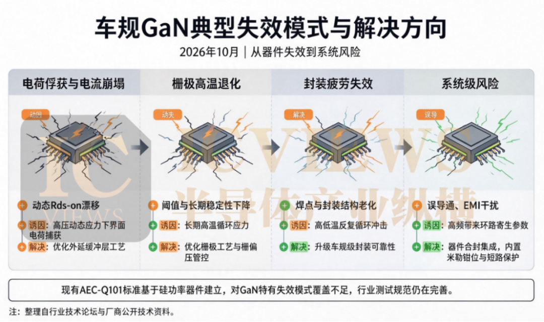
Even more troublesome is that the existing AEC-Q101 in the industry is built around silicon power devices and does not fully cover the dynamic failure of gallium nitride. In the testing system of silicon devices, many key failure modes are simply not applicable to gallium nitride, and there are no corresponding standard test items for the charge capture and dynamic drift unique to gallium nitride. Each device manufacturer and Tier1 can only supplement their own test items and test them separately, making it difficult to compare the results horizontally. That's why the verification cycle for automotive grade gallium nitride is often measured in years, as many testing standards are still struggling to cross the river.
Moreover, the high-frequency characteristics of gallium nitride pose new requirements for driver ICs, magnetic components, PCB layout, and EMI suppression. Simply replacing a gallium nitride device is not enough, and the entire power system solution needs to be iterated synchronously. No matter how good the performance of a tube is, if the driving circuit fails to keep up, the magnetic components do not match, and the PCB layout is not reasonable, the whole machine will still fail to produce results, and even reliability accidents may occur due to loop problems. This also explains why both InnoTech and NanoMicro need to develop integrated products. Essentially, manufacturers embed some of the system level anti-interference and protection capabilities into the devices, transferring the debugging pressure from Tier 1 to the device side, and using higher integration to lower the system landing threshold.
Gallium nitride is quietly entering the data center
If in car is currently the hottest main narrative of gallium nitride, then AI data centers are becoming its most underestimated increment. The AI wave has driven up the power consumption of computing clusters, with mainstream AI server cabinets increasing their power from 5kW in the early years to 40kW or even 60kW levels. The onboard and rack power supplies of servers have gradually shifted from traditional 12V architectures to 48V or even higher voltage HVDC high-voltage DC architectures. As soon as the voltage is raised, the shortcomings of silicon MOS in efficiency, power density, and heat dissipation are exposed. Test data shows that in the 48V to 12V onboard topology, the gallium nitride solution can improve the overall efficiency by 1.5 to 3 percentage points and power density by more than 40% compared to traditional silicon MOS, which is perfectly suitable for the demanding requirements of AI servers for power efficiency and power density.
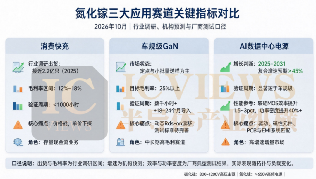
That's also why gallium nitride manufacturers are pushing hard towards this line. Nano Micro's GaN Safe and supporting solutions are heavily integrated into the power supply of AI servers, combining high-frequency gallium nitride with efficient topology to meet the cost per watt of data centers. InnoSeco is also laying out data center scenarios, extending its horizontal 650V and low-voltage product lines to the server power side simultaneously. On the industrial side, communication power supplies, energy storage converter branches, and AI onboard HVDC are generally considered to be markets with earlier volume than in vehicle models. This is because data center customers do not require an 18 to 24 month vehicle specification verification cycle like car manufacturers, making decisions faster and iterating more quickly. The verification and start-up pace of a power solution is much faster. According to institutional predictions, the global GaN power supply market for data centers is expected to grow at a rate of over 45% by 2026, making it the sector with the highest growth rate among all sub sectors.
From this perspective, the answer to whether gallium nitride can keep up with the AI wave is not just whether it can, but whether it is already on the way. The further AI develops and the higher the computing power density, the greater the power conversion pressure per unit area, and the clearer the demand for high-frequency, high-efficiency, and high power density gallium nitride. Gallium nitride is only focused on the power efficiency of data centers, rather than the spotlight position of computing chips. It is not under the spotlight, but almost every GPU server power board begins to have its presence. With the deployment of high-voltage bus architectures such as 800V and 48V in data centers, the presence of gallium nitride in the AI ecosystem is likely to continue to rise.
Looking at the timeline, the dividends of the fast charging track are cooling down, and the validation of new tracks such as in car and data centers has just begun. Gallium nitride is difficult to replicate the explosive path of the fast charging era, it is more like a slow and stable long-period power device business. In the next one or two years, the market will still focus on fixed-point verification and small-scale trial production, with limited revenue contribution. The high-volume carriers will be concentrated in 6.6kW on-board OBC, communication power supply, energy storage auxiliary branch, and data center onboard power supply. The mid-term focus is on continuously optimizing the stability of horizontal 650V integrated products, continuing to polish the substrate and epitaxial yield of vertical gallium nitride, and other economic turning points. The risks are also specific. The new generation of silicon MOS is still iterating and lowering prices, which will squeeze the cost-effectiveness window of gallium nitride; The verification cycle of vehicle regulations is long, and continuous product iteration and verification investment test the cash flow of enterprises, which not every company can withstand.
