


How do the three major local giants layout themselves in the face of mixed keys and the resurgence of turbulence?
As the miniaturization of advanced process transistors becomes increasingly expensive, relying solely on expanding chip area for computing power gradually encounters constraints in power consumption, yield, and cost. Engineers begin to re-examine the insignificant distance between chips.
As the number of stacked layers increases, these tiny metal structures will occupy more and more space, amplifying parasitic resistance, capacitance, thermal resistance, and interconnect density issues. Although chips can be stacked higher, signals need to pass through more connection structures.
The essence of hybrid bonding is to allow the copper pads of two wafers or chips to directly bite into the dielectric layer at the molecular level, skipping micro bumps and pressing the interconnect spacing within 10 microns.
The packaging of the convex dot era is like using a push pin to nail two sheets of paper together, while mixed bonding is like making two sheets of paper grow into one. It is the watershed between whether 3D stacking can go well or not.
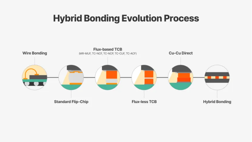
In August of this year, SK Hynix's technology column revealed typical technical scales, showing that the traditional solder ball interconnect spacing is about 100 microns, micro bumps are about 20 microns, and hybrid bonding can reduce the interconnect spacing to below 1 micron.
The changes in size far exceed the range that can be understood by the naked eye, but are enough to rewrite the internal traffic rules of high-performance chips.
Higher interconnect density means more data channels, and shorter connection paths are beneficial for reducing signal loss and transmission delay.
For high bandwidth memory HBM, 3D NAND, CMOS image sensors, and Chiplet heterogeneous integration, these changes directly affect the performance, power consumption, and stacking capability of the product.
The technical value of hybrid bonding has been proven, but the most exciting incremental market has not yet completed the process route switch.
Tiny particles, copper pad indentations, wafer warping, or local deformation can all cause interface voids, misalignment, and electrical connection failure.
A competition about connecting devices is turning into a competition for process chain control capabilities.
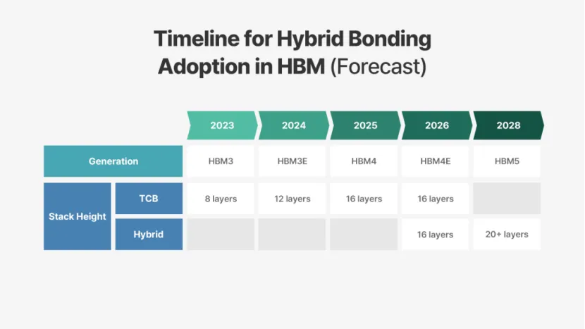
In July 2026, it was revealed that Samsung and SK Hynix would temporarily not introduce hybrid bonding in HBM4 and would continue to use mature hot press bonding, at the earliest until the HBM4E generation.
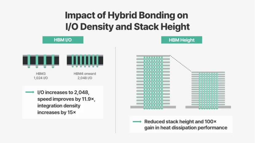
The trigger was quite subtle. JEDEC relaxed the upper limit of HBM packaging height from 775 microns to 1000 microns, and the 12 layer stack no longer reached the ceiling at once, dissipating the urgency of the new technology.
Delay does not equal rejection. The number of I/Os in the HBM5E generation will double from 2048 to 4096, and the physical limit of bump spacing is there. Stacks with more than 16 layers will ultimately not be able to bypass hybrid bonding.
TSMC's SoIC, 3D NAND wafer to wafer stacking, and CIS three-layer structure are all advancing at their own pace.
According to Yole Group's calculations, hybrid bonding equipment is the fastest-growing segment in the aftermarket, with a compound annual growth rate of 21.1%. The market size is expected to reach 397 million US dollars by 2030, and the combined market growth of hot press bonding and hybrid bonding will reach approximately 1.3 billion US dollars by 2030. The overall market for high-end packaging will exceed 51 billion US dollars by 2031, nearly five times the level of 2025.
The delay of overseas manufacturers has precisely extended the verification window for domestic equipment by one to two years. Currently, Dutch manufacturer BESI holds approximately 70% of the global market share in hybrid bonding equipment, demonstrating an absolute leading position.
For Chinese equipment manufacturers, this unexpectedly relaxed time difference is the premise of the entire story.
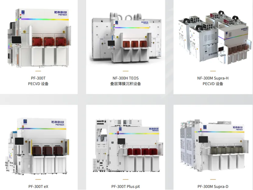
Tuojing Technology: Install the entire bonding production line into the product catalog
Among the three companies, Tuojing is the only one that generates real gold and silver income through mixed bonding.
In 2025, the company's hybrid bonding equipment achieved a revenue of 136 million yuan, a year-on-year increase of 41.92%. Wafer to wafer hybrid bonding products continued to receive orders, and multiple devices passed customer verification. The first wafer to wafer fusion bonding product also achieved revenue conversion. 136 million yuan only accounts for about 2% of the total revenue of 6.519 billion yuan, but its structural significance is far greater than its proportion.
Tuojing started laying out 3D integration in 2018, and now the product catalog reads like a list of equipment for a bonding production line.
The Dione 300 wafer to wafer hybrid bonding equipment has received duplicate orders, and the new generation of high-speed and high-precision products have been validated for shipment; Low stress melt bonding equipment Dione 300F targets advanced logic; The chip to wafer hybrid bonding device Pleione is currently undergoing validation on the client side.
Propus 300 is responsible for surface activation and cleaning before bonding, Crux 300 is responsible for measuring registration accuracy after bonding, Ascella 300 detects bonding strength, Lyra processes laser peeling, and the bonding accuracy of the entire equipment can reach hundreds of nanometers.
The enemy of mixed bonding mass production yield is distributed in every process before and after the bonding action, with particles, warping, alignment, and measurement. Any loss of one link will turn copper to copper perfect bite into a yield black hole.
Tuojing's sales to customers are a closed-loop process centered around bonding, which has upgraded its bargaining method on the client side from selling individual machines to selling production lines.
The thickness of the main business has given enough patience to this second curve. In 2025, Tuojing PECVD equipment revenue was 5.142 billion yuan, a year-on-year increase of 75.27%. The net cash flow from operating activities was 3.633 billion yuan, and the year-end orders were about 11 billion yuan. The acquisition of Wuxi Shangji is still strengthening the PVD process.
Thin film deposition supports the family, three-dimensional integration strategizes, and the bonding story of Tuojing tells a story of both food and grass.
Northern Huachuang: 405 million yuan to buy admission tickets for time-based payment
Northern Huachuang is the king of domestic equipment in terms of volume, with a revenue of 39.353 billion yuan in 2025, a year-on-year increase of 30.85%.
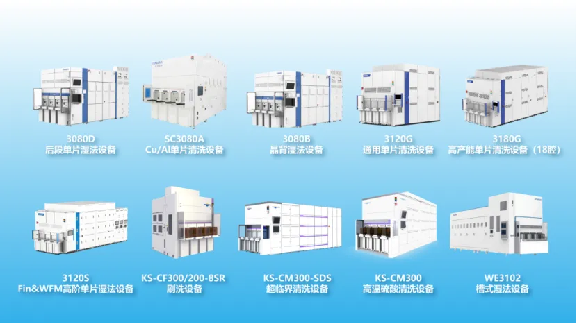
Platformization is its keyword, and its product line ranges from etching and thin film deposition to furnace tubes, cleaning, and ion implantation. In March 2026, it also released the 12 inch chip to wafer hybrid bonding equipment Qomola HPD30, Gluoner R50 bonding equipment for 3D NAND and DRAM, and the first electroplating equipment.
After controlling Xinyuan Microelectronics, the total wet process coverage of both parties exceeds 97%. The 2026 semi annual report shows that its hybrid bonding equipment has completed client verification and obtained bulk orders.
Self research is on the way, but Northern Huachuang still chooses to spend another 405 million yuan to acquire Novokey. This target has only been established for one and a half years, with a revenue of 19.1768 million yuan and a net loss of 29.8761 million yuan in 2025. Its operating income in the first half of 2026 will be zero, with an income based valuation appreciation rate of 27.04%.
On the books, this is a loss making transaction. Strategically, what North Huachuang is buying is very clear, including a mature R&D team, a complete intellectual property package, duplicate orders that have already been received, and an ongoing verification channel for top customers.
The seller equipment phase II fund of the transaction structure is funded by affiliated parties of North Huachuang, incubated first, and taken over by the listed company at an appropriate time. It has a unique seedling transplanting process of the state-owned asset system. The confirmation of mixed bonding equipment from factory entry to mass production is often measured in years.
The revenue volume of 39.3 billion yuan allows Northern Huachuang to compress a portion of this period with 405 million yuan. This is the privilege of platform companies, but also hides their anxiety. The self-developed HPD30 and the acquired Novokey are destined to compete internally on the same production line.
Zhongwei Company: Surrounding the bonding machine with a massive system
Zhongwei's posture seems the most conservative, but upon careful consideration, it is the most shrewd. In 2025, the company's revenue will be 12.385 billion yuan, a year-on-year increase of 36.62%, and research and development investment will exceed 3.7 billion yuan. It did not announce the production of a complete bonding machine, only did three things.
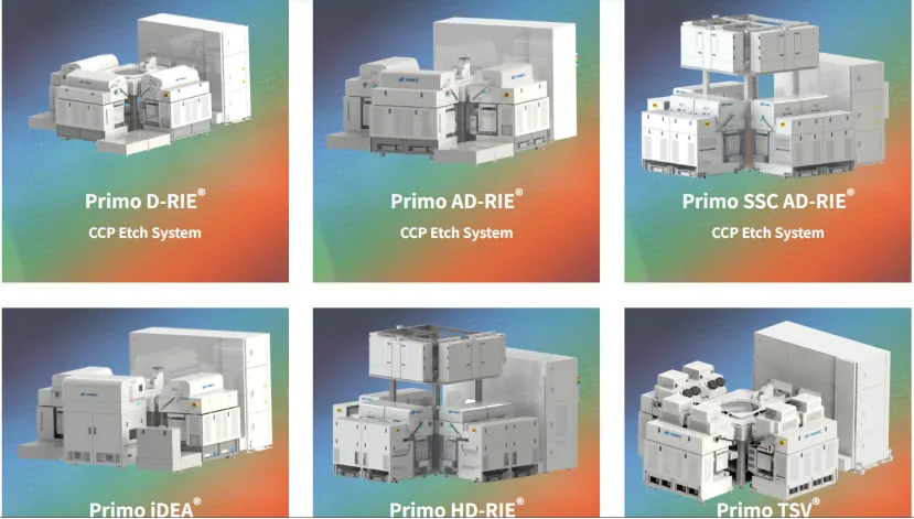
① The Primo TSV 300E continues to serve customers and has received repeated orders by achieving the ultimate etching of TSV deep silicon through holes. It has completed the development of 12 inch high aspect ratio deep trench capacitor etching and SoIC wafer to wafer processes, and successfully verified them on top domestic customer production lines. The third-generation TSV etching machine is also on the way.
② Surrounding advanced packaging, the development of CuBS PVD integrated equipment has been smooth, and plasma cutting equipment Primo Matrix has negotiated with multiple important customers for etching CVD、PVD、 The quantity testing covers the entire line.
③ Increase the capital of Qinghe Jingyuan by no more than 35 million yuan, with a pre investment valuation of 6.75 billion yuan, holding SAB82 chip to wafer hybrid bonding equipment, supporting high-density interconnect spacing of less than 10 microns, and generating revenue of 93.7332 million yuan in 2025.
Zhongwei is well versed in the iron laws of the equipment industry. The bonding machine is just a corner of the mixed bonding production line exposed to the water, and beneath the water surface is a massive system consisting of activation, cleaning, etching, deposition, and measurement.
Catch the surrounding processes one by one, whether to do or not to do the bonding machine, and always hold the initiative in your own hands.
At the end of the window period, there is a validation competition that no one can lose.
Put the three companies on one picture, and the shape of domestic mixed bonding will be clear.
Explore the depth of Jingwei gambling and launch a frontal attack with a full chain product matrix.
The Northern Huachuang Gambling Platform is advancing through both self-developed and mergers and acquisitions, trading volume for time.
Zhongwei Gambling Ecological niche, holding onto the main channel of etching, using small equity investments to occupy options.
In the periphery, Huahai Qingke has also entered the thinning process, while equipment from Maiwei Group and Baiao Chemical has entered industrialization verification. The entire domestic camp has shown a group charging trend that has not been seen in many years.
3D NAND and image sensors have formed a mature application foundation, and some logic chips have also been commercialized.
HBM still needs to address manufacturing costs, thermal management, yield, and equipment capacity issues at higher stacking levels.
At a stage where traditional hot press bonding technology can still meet production requirements, storage manufacturers have no incentive to immediately replace the entire manufacturing process just for the sake of technological advancement.
This means that hybrid bonding equipment companies need to simultaneously handle order competition in mature application markets, as well as customer certification for new applications such as next-generation HBM, 3D DRAM, Chiplets, etc.
At the same time, overseas equipment manufacturers such as EV Group, Besi, ASMPT, etc. continue to promote cooperation in hybrid bonding related technologies and industries.
In 2025, ASMPT and Kokusai Electric announced a joint development of hybrid bonding and micro bump hot press bonding technology solutions, emphasizing the synergy between thin film materials, bonding equipment, and processes.
Ending
In the second half of chips, it's no longer just about who cuts the line width finer, but also who stacks the chips denser. Hybrid bonding has pushed packaging from the latter supporting role to the main position of the manufacturing process.
After semiconductor manufacturing entered three-dimensional space, the connection between chips also became the battlefield that determines performance and cost.
