


TSMC A14 process breaks through SRAM miniaturization stagnation for eight years: storage cell area drops to below 0.017 square micrometers
As the world's largest and most advanced semiconductor manufacturer, TSMC's progress in SRAM miniaturization has been stagnant for many years. Since the mass production of N5 (5 nanometers) process in 2020, the area of its high-density 6T SRAM storage unit has remained at about 0.021 square micrometers. Although the N3 and N2 nodes continue to iterate on logic transistors, the size of the storage unit has remained almost unchanged. This situation is expected to be broken with the arrival of the A14 node: TSMC plans to reduce the area of high-density 6T SRAM bit cells to less than 0.017 square micrometers in the A14 process that will be mass-produced in 2028, a decrease of more than 19%.
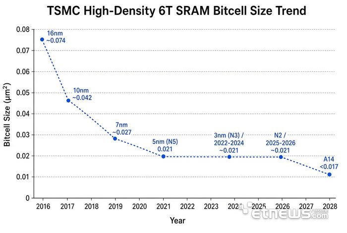
Reviewing the evolution trajectory of TSMC's high-density 6T SRAM bit cell area: in the 16nm era, it was about 0.074 square micrometers, in the 10nm era, it decreased to about 0.042, in the 7nm era, it further decreased to about 0.027, and in the N5 (5nm) era, it reached about 0.021 square micrometers. However, since the mass production of N5 in 2020, this number has not changed significantly in the N3 (2022-2024) and N2 (2025-2026) eras, forming a "horizontal line" that lasts for about eight years.
The reason why SRAM miniaturization has fallen behind is related to its physical characteristics. A 6T SRAM cell uses six transistors to store one bit, and must maintain sufficient read and write stability and reliability at a smaller size. Advanced technology does not necessarily mean that the storage cell can be reduced in size. The consequence is that cache increasingly occupies a larger proportion of advanced chips, and chip costs and size pressures continue to rise.
Unit area reduced by over 19%
According to TSMC's paper abstract submitted to the IEDM (International Electronic Devices Conference) in December 2026, the A14 NanoFlex Pro platform will feature the "world's smallest SRAM" with a cell size of less than 0.017 square micrometers and achieve the highest SRAM macro density to date through size scaling rules.
Calculated from 0.021 to less than 0.017, the reduction in unit area is slightly over 19%, and theoretically the number of units that can be accommodated per unit area increases by over 23.5%. However, it should be noted that the reduction in cell area does not equate to a year-on-year increase in complete memory density - SRAM macros also include peripheral circuits such as decoders and sense amplifiers, and the actual density gain depends on the degree of reduction of these auxiliary circuits. Previously, it was reported that according to the currently disclosed data, the SRAM cell area of A14 is expected to lead Intel's 18A process (its announced high-density SRAM cell area is 0.021 square micrometers); Samsung has not yet disclosed the latest SRAM cell size technology, so it is currently not possible to directly compare.
Trial production is underway, with pre production in 2027 and mass production in 2028
In addition to SRAM, A14 is TSMC's second-generation GAA nanosheet transistor process after N2, and is equipped with the NanoFlex Pro standard cell architecture. The official goal set by TSMC is to increase speed by 10% to 15% or reduce power consumption by 25% to 30% and increase chip density by approximately 20% compared to N2 at the same power consumption.
In terms of progress, TSMC disclosed during its financial conference call in July 2026 that its internal "product like" validation vehicles have demonstrated device performance of nearly 90%, with a 256Mb SRAM yield rate of nearly 90%. Customer chip out activities have started and progress is earlier than originally planned.
Currently, TSMC is conducting trial production to evaluate the feasibility of the nodes and allow customers to verify the actual performance of their own designs. The official schedule is to start pre production (risk trial production) in 2027 and enter mass production in 2028. The IEDM summary also confirms that A14 is "proceeding with mass production in 2028 as planned".
There are market reports that, given the smooth progress in the early stages, there is a possibility of advancing the schedule by several months. However, according to sources cited by Futu Community, TSMC has not officially confirmed this acceleration schedule. According to cnBeta, A14 will be the first to enter mass production at TSMC's headquarters in Taiwan. In addition, TSMC is expected to release relevant research results by the end of this year.
Can on-chip caching alleviate AI data bottlenecks?
SRAM is a key component for the internal cache of CPUs, GPUs, and AI acceleration chips. After shrinking the unit, the same chip area can accommodate more cache, which helps alleviate the data access bottleneck of AI chips and improve performance and energy efficiency; For AI accelerators, larger on-chip storage may also reduce the frequency of access to external HBMs. Of course, a larger cache does not automatically equate to higher performance, and the actual benefits still depend on latency, bandwidth, and access modes, and the yield of the 256Mb experimental structure is not equal to the yield of the complete chip. The final outcome still needs to be verified based on yield, cost, and customer adoption.
