


Abandoning SRAM for 3D Stacked DRAM: NVIDIA and Groq's Next-Generation Architecture Gamble
After Nvidia's substantial $20 billion acquisition of Groq, its next-generation LPU chip architecture plans to abandon SRAM and shift to 3D stacked DRAM (3DS), using TSV vertical interconnect to expand capacity while maintaining standard DRAM interfaces. Its 500MB SRAM is only 1/500 the capacity of Rubin HBM, unable to support hundreds of billions of models. The memory tier of AI inference chips is moving toward hybridization.
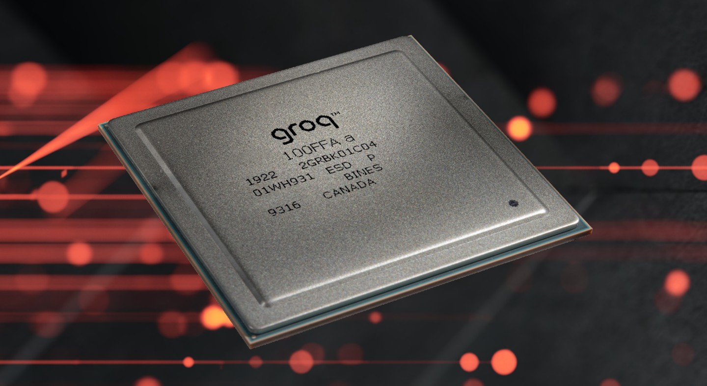
The first heavy blow after $20 billion: the rapid shift from SRAM to 3DS architecture. Signals of a dramatic architectural transformation are emerging in the AI semiconductor field. According to Korean media outlet ZDNet Korea, citing semiconductor industry sources, Groq, an AI chip company substantially acquired by Nvidia, is considering abandoning the SRAM solution used in its next-generation chips in favor of 3D stacked DRAM packaging technology.
The background of this deal is worth reviewing. Groq was founded in 2016 by Jonathan Ross, the designer of Google's TPU, and was indirectly acquired by Nvidia in December 2025, signing a technology licensing agreement. The deal is worth about $20 billion, marking the largest move in Nvidia's 32-year history—far surpassing the $6.9 billion acquisition of Mellanox in 2019; The brilliance lies in its structural design: NVIDIA did not fully acquire Groq, but acquired its inference chip technology through a "non-exclusive technology licensing agreement," bringing founder Jonathan Ross and the core team under its umbrella. Groq itself continues to operate independently—this arrangement not only avoids potential antitrust issues but also completes technology absorption. According to SEMI data, by 2026, inference computing power will account for over 70% of global AI infrastructure for the first time, and Nvidia's share of the inference chip market has climbed from 66% to 74%—extending from training to inference is the strategic foundation of this deal.
Now, the first architectural move after the acquisition has taken a surprising direction. Currently, most AI chips use 2D packaging. Groq plans to introduce 3D packaging to vertically stack multiple semiconductor dies, with a solution called 3DS (3D Stacked Memory)—using TSV (Through-Silicon Via) technology to drill thousands of micro-holes inside DRAM chips for vertical interconnection, like constructing skyscrapers for memory or connecting layers via vertical elevators, providing memory density far beyond traditional designs per unit area. According to industry insiders, this is about making chips "grow upward like building blocks," improving power transmission efficiency and storage capacity while maintaining a small chip area.
The limits of SRAM: The huge gap between 500MB and 288GB
To understand this shift, we first need to understand Groq's previous foundation. Groq's LPU (Language Processing Unit) architecture is renowned for extremely fast inference: the current flagship Groq 3 LPU uses a large-capacity SRAM design, with each chip integrating about 500MB of on-chip SRAM and a maximum memory bandwidth of 150TB/s. Korean media outlet TheElec claims this is 7 to 45 times faster than HBM. Technically, SRAM's access latency is not "slightly faster" than DRAM, but an order of magnitude faster—typical HBM/DRAM latency is about 100 nanoseconds, while SRAM only needs 1 nanometer. When model weights reside directly in SRAM, there is no need for caching guessing or waiting, and latency bottlenecks are physically broken. At the system level, NVIDIA's Groq3 LPX rack released at GTC 2026 adopts a fully liquid-cooled design and MGX infrastructure, integrating 256 LPUs, 128GB of on-chip SRAM, corresponding to 40PB/s of SRAM bandwidth, positioned as an AI inference accelerator on the Vera Rubin platform, which can increase inference throughput supported by up to 35 times per megawatt of power.
But SRAM's strength lies in speed, but the trade-off is capacity, cost, and chip area. SRAM units have complex structures, large silicon footprint, high unit capacity costs, and scaling is nearing its limit—in TSMC's 5nm to 3nm process evolution, compute units can shrink by about 1.6 times, while SRAM unit area is only about 5% smaller. The contrast is very clear: Groq 3's roughly 500MB SRAM capacity is only 1/500 of Nvidia's Rubin GPU with a single 288GB HBM4 chip; To run trillion-parameter large models solely on an LPU, thousands of chips must be connected in parallel, significantly reducing chip-level token processing efficiency. Nvidia's current transitional approach is system-level complementarity—pairing the Groq3 LPX rack and Vera Rubin GPU via Spectrum-X interconnect, with the high-bandwidth LPU handling feedforward network layer computation and the GPU handling the attention layer requiring large key-value memory. The next-generation chips directly shifting to 3D stacked DRAM are attempts to expand capacity at the chip level and break through SRAM bottlenecks.
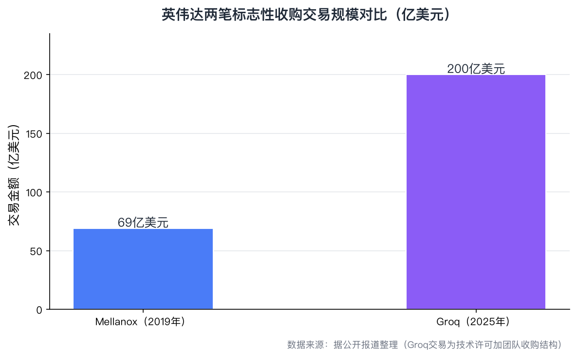
[Chart: Comparison of Scale of Two Iconic Acquisition Deals by Nvidia]
Chart Interpretation: From $6.9 billion to $20 billion worth of Groq, Nvidia's largest acquisition record has nearly doubled—the strategic importance of the deductive era is now on par with network interconnection technology back then.
The collective shift of the major SRAM genre: The same choice among three companies
Groq's shift is not an isolated event but a microcosm of industry consensus.
Cerebras, also known for its large SRAM route, announced at Hot Chips 2026 that the future CS-6 system will introduce wafer-level 3D stacking for the first time, placing the DRAM layer vertically interconnected over logic and SRAM wafers via ultra-high bandwidth, maintaining the advantage of low-latency near-memory computing while breaking the bottleneck of relying solely on SRAM expansion. According to its official technical blog, CS-6 integrates wafer-level SRAM with computing power and 3D stacked DRAM, aiming to significantly expand memory capacity "without sacrificing the local advantages of wafer-level speed." The company also simultaneously announced the Nexus system architecture and multi-generation roadmap—CS-5 aims for a generation speed of 10,000 tokens per second per user in 2027, while CS-6 will be the first to stack DRAM directly on top of computing wafers.
AI inference chip company d-Matrix went even earlier. In November 2025, d-Matrix and Alchip announced a collaboration to develop the world's first 3D stacked DRAM solution for AI inference, claiming inference speeds could reach up to 10 times that of HBM4; Its Raptor solution uses an architecture where TSMC N4 logic dies and 3D DRAM dies are stacked face-to-face. In silicon area benchmarks, the bandwidth per unit area reaches 32.6GB/s/mm², about 20 times that of HBM4 and NVIDIA Rubin R200, with bandwidth power consumption of only 2.96 milliwatts per GB/s, a 13.5-fold improvement over HBM, and single-card bandwidth exceeding 100TB/s. Its CEO clearly stated: "This is not a traditional HBM solution." On the system product side, its current Corsair accelerator is equipped with 2,048 digital memory compute cores, 150TB/s performance memory bandwidth, and up to 256GB of memory.
The three major SRAM schools are simultaneously heading in the same direction—from SRAM alone to a hybrid memory tier called "SRAM + 3D stacked DRAM."
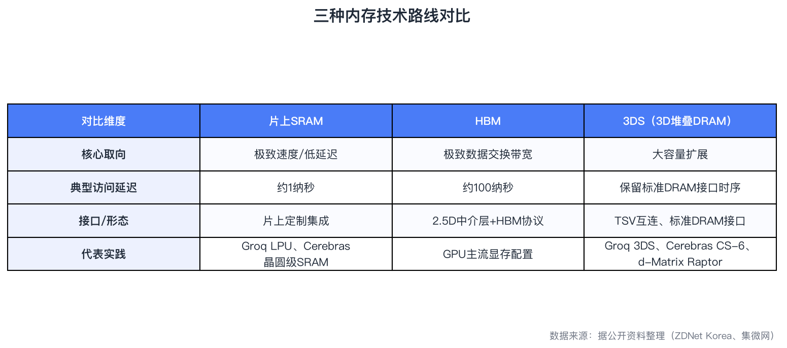
[Chart: Comparison of Three Memory Technology Routes]
Chart Interpretation: Although DRAM's native read/write speed is slightly slower than SRAM's, its large capacity gives it an advantage in complex model deployments—for AI inference tasks that require massive parameters, 3DS focuses on capacity expansion while maintaining the standard DRAM interface protocol, making it a more practical cost-reduction and efficiency improvement solution than HBM.
The logic behind this is not complicated. The entire market is evolving toward "larger chips," and choosing DRAM with higher capacity is in line with this trend; Looking deeper, HBM's speed dividend is approaching physical limits, and the industry's previous common choice was to "make SRAM bigger"—NVIDIA significantly expanded on-chip SRAM capacity and maximized compute unit bandwidth during the Rubin design phase. But SRAM's density gain ultimately cannot keep up with the expansion rate of model parameters: in TSMC's 5nm to 3nm process evolution, compute units can shrink by about 1.6 times, while SRAM unit area is only about 5% smaller. When SRAM scaling hits a ceiling, 3D stacked DRAM becomes the optimal solution between "near-memory computing" and "large capacity": maintaining low latency while accommodating models. ZDNet Korea cited another industry insider's analysis that the entire market is evolving toward "larger chips," and Groq's choice of higher-capacity DRAM is in line with this trend.
Industry impact: The memory hierarchy reconstruction
of the inference era has shifted this architecture into a broader industry landscape, showing three layers of significance.
First, inference is defining new competitive rules. The rapid development of generative AI has made inference a new competitive frontier—inference places greater emphasis on throughput, latency, and energy efficiency, driving the rise of ASIC chips like Google's TPU, with TPU shipments increasing significantly since 2025.
Groq's LPU architecture emphasizes high-speed token output and real-time responsiveness, complementing GPUs; According to analysis by Korea's IM Securities, LPUs can achieve response speeds about 10 times faster than traditional GPUs and over 90% higher energy efficiency. Their deterministic scheduling design allows multiple chips to interconnect and operate like a single giant core. Acquiring Groq means NVIDIA has built defenses in advance on the new inference battlefield.
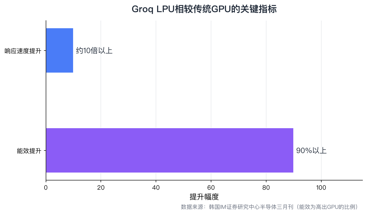
[Chart: Key Metrics of Groq LPU Compared to Traditional GPUs]
Chart Interpretation: Over 10 times faster response speed and over 90% higher energy efficiency are the foundation for LPUs to establish themselves in low-latency inference scenarios—and for next-generation architectures to maintain these two metrics, the biggest challenge in shifting to 3D stacked DRAM is to maintain these two metrics.
Second, the memory hierarchy is moving towards hybridization. Using Groq's technology, NVIDIA can build a hybrid memory architecture where "high-capacity data is handled by HBM/DRAM, and real-time high-speed computing is handled by SRAM"—this echoes the custom trends in the HBM field. NVIDIA's NVHBM custom HBM, released in August, also lowers the memory controller to the base die, redefining the division of labor among GPU, HBM, SRAM, and 3D-stacked DRAM. It's worth noting that the Groq3 LPU chip is currently fabricated with Samsung's 4nm process. Jensen Huang publicly confirmed at GTC 2026 that "Samsung is manufacturing Groq3 chips for us." Supply chain sources indicated that Groq's existing chips have already been produced with Samsung's 4nm process, and the current collaboration merely continues the existing product line.
Third, the battle for ecosystem influence has extended to storage standards. The 3DS design retains the standard DRAM interface, allowing it to access the mature DRAM ecosystem without starting from scratch. If Groq's next-generation chips successfully validate this path, "SRAM for compute-level cache and 3D-stacked DRAM for capacity" could become a reference architecture for inference chips, introducing new variables for DRAM manufacturers, TSV packaging capacity, and HBM supply and demand.
Future Outlook: Three Observations in the Era of Hybrid Memory Hierarchies
Looking ahead to the next-generation Groq chips, there are three key observations. First, the 3DS solution's production schedule and yield—TSV technology, which penetrates thousands of microvias in DRAM, is complex, and whether the balance between capacity and speed can fulfill the expectation of "maintaining a speed advantage while addressing capacity shortcomings" remains to be tested. Second, the implementation difficulty of hybrid memory hierarchy in the software stack—from SRAM-only to coordinated SRAM and 3D DRAM, compilers and scheduling strategies need to be rewritten, which is precisely where the LPU's "deterministic execution" concept comes into play and also represents the greatest engineering risk. Third, NVIDIA's self-development pace—their self-developed 3nm base die and custom HBM (NVHBM) are already underway, and how Groq's 3DS path coordinates with this will determine the completeness of NVIDIA's "GPU-LPU-Custom Storage" full stack.
The bigger picture is this: as inference computing power accounts for more than 70% of global AI infrastructure, storage—rather than computing power—is becoming the main battlefield for AI chip innovation. From the hybrid bonding of HBM4 to the custom base of NVHBM, and then to Groq's 3DS, a clear evolution path emerges: whoever can use the lowest energy to "pack the largest models into the storage closest to computing" will control pricing in the AI inference era. NVIDIA and Groq's recent architectural shift is just the latest shot in this battle.
