


New solution for HBM heat dissipation: SK Hynix launches iHBM technology, reducing embedded component thermal resistance by 30%
Recently, SK Hynix is in close contact with upstream and downstream partners to accelerate the mass production process of its next-generation high bandwidth memory cooling technology - iHBM (Integrated Cooling HBM). This highly anticipated technology in the industry has successfully reduced thermal resistance by over 30% by embedding dedicated cooling elements (ICE) inside the package.
In today's era where the parameters of AI models are growing exponentially and the demand for computing power is almost bottomless, this breakthrough is not only a simple process improvement, but also a key winner in determining the high-performance computing landscape for the next five years. It marks the competitive dimension of HBM, which has officially entered a new deep-water area of "package level thermal architecture" from the simple "stack height" and "transmission bandwidth".
The heating problem brought by the soaring computing power of AI
To understand the strategic value of iHBM, we must first face the severe physical challenges facing the current AI infrastructure. Since the outbreak of generative AI in 2023, HBM, as the core component to break the "memory wall", has risen from supporting role to the leading role. However, with the popularization of HBM3E and the successive implementation of HBM4 and HBM5 standards, the stacking layers of a single chip have increased from 8 to 12 or even 16 layers, and the data transmission rate has exceeded 10Gbps pin rate. Along with this, there has been a sharp surge in power consumption and heat generation.
In traditional architecture, the heat dissipation of HBM mainly relies on external heat sinks, thermal interface materials (TIM), and system level air cooling or liquid cooling. This passive heat dissipation mode of "from outside to inside" can still be barely maintained in the HBM3 era, but it has shown signs of fatigue when facing the HBM5 and higher generations. The reason is that HBM adopts silicon via (TSV) vertical interconnect technology, and the heat is not evenly distributed, but highly concentrated in the D2D PHY (Die to Die Physical Layer) interface area.
This logic layer located at the bottom of the stack is the throat for data entry and exit, and also the hottest "hotspot" in the entire package. When external cooling methods cannot effectively penetrate dozens of layers of silicon wafers to reach the core hotspot, thermal accumulation can lead to a decrease in signal integrity, an increase in leakage current, and even trigger frequency down protection mechanisms. For AI data centers that pursue ultimate energy efficiency, this means that expensive GPU computing power is forced to idle, and system stability faces huge risks.
Thermal management has evolved from an auxiliary engineering problem to a physical ceiling that constrains the continuation of Moore's Law and the release of AI computing power. Whoever can first solve the "hot congestion" within HBM has the right to define the next generation of AI chips.
The internal heat dissipation principle of iHBM technology
The iHBM technology launched by SK Hynix is essentially a paradigm shift in the philosophy of heat dissipation. It is no longer obsessed with how to quickly remove heat from the packaging surface, but is committed to building a low resistance heat dissipation highway inside the packaging. The core carrier of this technology is ICE (Integrated Cooling Element). Unlike traditional metal heat dissipation covers, ICE is a specialized component made of insulating and highly thermally conductive silicon-based materials.
The choice of silicon-based materials instead of copper or aluminum reflects SK Hynix's profound packaging process considerations: the coefficient of thermal expansion (CTE) of silicon and HBM chips is perfectly matched, which can completely avoid stress warping and reliability hazards caused by heterogeneous material bonding; Meanwhile, its excellent insulation properties allow the component to be directly embedded in densely populated areas of the circuit without worrying about the risk of short circuits.
In terms of structural design, iHBM precisely embeds ICE components into the D2D PHY area where heat is most concentrated, which is equivalent to opening a "window" directly to the outside next to the "furnace" of the chip core. This built-in hot channel bypasses the stacked DRAM chips, exporting the heat generated by hotspots to the top of the package in the shortest path and with the lowest thermal resistance, and then passing it on to the system level heat sink for processing.
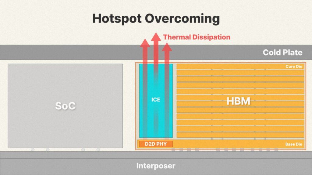
SK Hynix announces iHBM concept map (Image source: SK Hynix)
Test data shows that compared to traditional solutions, iHBM can reduce overall thermal resistance by more than 30%. This 30% reduction, in thermodynamic terms, means that the junction temperature can be reduced by 10-15 degrees Celsius under the same power consumption, or the power consumption can be increased by more than 20% under the same temperature budget - this is a real increase in computing power for AI accelerators that are expensive.
More importantly, iHBM is not a disruptive design that requires a complete overhaul, but rather an incremental innovation based on SK Hynix's mature MR-MUF (Mass Reflow Molded Underfill) process. This means that existing GPU and ASIC customers can seamlessly import this technology without changing the motherboard layout, redesigning sockets, or undergoing lengthy system level revalidation. This "backward compatibility" engineering wisdom greatly reduces customers' migration costs and paves the way for iHBM's rapid commercialization.
Supply chain integration and mass production preparation
Although the progressiveness of technology is important, whether it can be transformed into large-scale mass production products is the only criterion to test commercial success. The reason why the news on October 22, 2026 has attracted high market attention is precisely because SK Hynix's actions have moved from the technology research and development stage to the substantive stage of supply chain integration and mass production preparation.
According to reports, SK Hynix has recently had intensive discussions with upstream partners in materials, components, and equipment at home and abroad, covering specific topics such as material supply of ICE components, precision machining equipment, packaging production line transformation, and yield improvement plans. This indicates that iHBM is no longer a concept on PPT, but has entered the practical stage of BOM list and production scheduling. Considering that HBM5 is expected to enter the mass production cycle around 2027, the current supply chain integration is aimed at ensuring precise alignment between production pace and customer demand.
This action also sends a strong industry signal: SK Hynix is building an exclusive ecological barrier around iHBM. By locking in the production capacity of key materials and equipment in advance and conducting joint verification with core customers, SK Hynix is actually defining the heat dissipation standards for the next generation HBM.
While competitors are still exploring external heat dissipation optimization solutions, SK Hynix has turned "built-in heat dissipation" into a de facto industry benchmark. For downstream GPU manufacturers, once they become accustomed to the thermal design margin and system simplification brought by iHBM, their willingness to switch back to traditional solutions will significantly decrease. This path from technological leadership to customer stickiness is the deep logic behind SK Hynix's long-term market share leadership in the HBM market.
Changes in Competitive Landscape and Future Prospects of Computing Power
In the three game battle of HBM market, the competition between Samsung, Micron, and SK Hynix has long focused on bandwidth, capacity, and yield. However, as companies gradually converge on basic specifications, the focus of differentiated competition will inevitably shift towards deeper physical characteristics. The emergence of iHBM marks that heat dissipation capability has officially become a new dimension of competition for HBM.
For Samsung, its profound accumulation in the field of advanced packaging cannot be underestimated, but the MR-MUF process and ICE integration solution that iHBM relies on are unique know-how developed by SK Hynix through years of iteration. If Samsung wants to follow up, it not only needs to overcome similar embedded heat dissipation technologies, but also needs to rebuild a matching supply chain system, and the time window is narrowing. Although Micron has won a reputation for its low power consumption on HBM3E, in the ultra-high density stacking scenario for HBM5, relying solely on process advantages is difficult to completely offset the heat accumulation effect, and it also needs to come up with its own package level heat dissipation solution.
The more profound impact is that iHBM may change the design methodology of AI chips. In the past, chip architects often needed to reserve sufficient thermal design margin for HBM when designing GPUs or ASICs, which to some extent limited the performance release of computing cores. When HBM has efficient built-in heat dissipation capabilities, the system level thermal budget can be allocated more to computing units, thereby achieving a significant increase in overall computing power. In other words, iHBM is not only saving HBM itself, but also unleashing the performance potential of the entire AI accelerator.
Since the first generation HBM was introduced in 2013, high bandwidth memory has undergone more than a decade of evolution. The breakthroughs of each generation of products are the result of humanity's game against physical limits at the atomic scale. When the stacking layers approach the boundary of mechanical stress and the transmission rate approaches the limit of signal integrity, heat dissipation becomes the next fortress that must be overcome. The advancement of SK Hynix iHBM technology is the latest footnote to this game.
It tells us that in the post Moore era where Moore's Law slows down, innovation no longer comes solely from the miniaturization of transistor sizes, but also from the systematic reconstruction of interdisciplinary fields such as packaging, materials, and thermodynamics. Embedding heat dissipation components into chips may seem like a minor structural change, but it actually represents a profound transformation of the semiconductor industry from "flat thinking" to "three-dimensional system integration thinking".
