


The Xtacking architecture of Chinese manufacturers is truly a 'nuclear weapon' for storage chips!
Recently, some media have reported that Changjiang Storage is entering the DRAM memory field and will apply its Xtacking architecture to DRAM memory to carry out dimensionality reduction efforts.
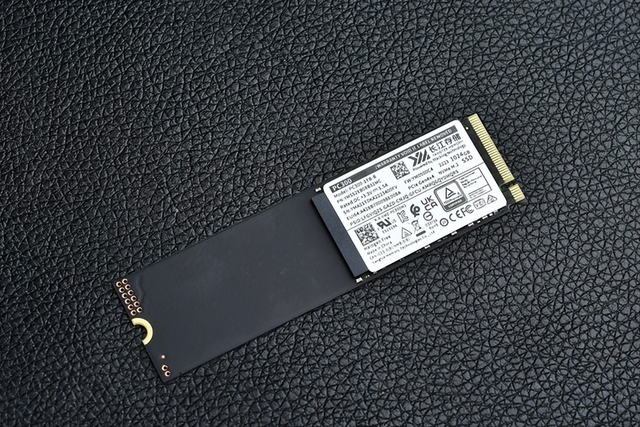
Regarding the Xtacking architecture, many people may not be very clear about it. Changjiang Storage refers to it as "crystal stack", which is the core patent of Changjiang Storage. This technology is integrated with hybrid bonding technology.
We know that logic chips are all composed of transistors. The more transistors there are, the smaller the transistors, and the stronger the performance. Therefore, there are miniaturization technologies for transistors such as 7nm, 5nm, 3nm, and 2nm, which are becoming smaller and smaller.
But storage chips are different from logic chips. Storage chips are composed of a transistor and a capacitor, and data is stored in the capacitor. The smallest unit is a 1T1C structure and is not entirely composed of transistors.
At the same time, storage chips cannot be physically miniaturized continuously. Manufacturers have found that when the miniaturization reaches a certain level, such as before and after 15nm process, further miniaturization can lead to instability of the storage chip, which is a major taboo for storage chips.
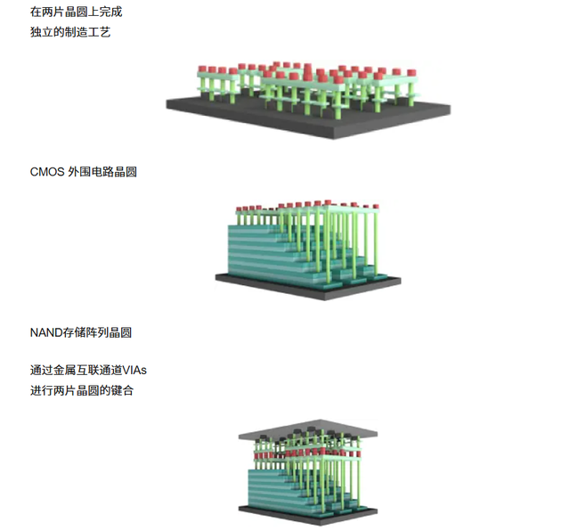
We need to improve the craftsmanship again, but we can't do miniaturization anymore. What should we do? So Changjiang Storage came up with a solution. Since the storage chip consists of storage units and peripheral circuits, the storage units cannot be continuously miniaturized, but the peripheral circuits can be processed separately and then combined together.
This is called "Xtacking", which realizes the processing of peripheral circuits and storage units on two independent wafers. The storage units can be manufactured using stable processes, but the peripheral circuits can be manufactured using advanced processes without affecting each other. After each processing is completed, the two are bonded together using hybrid bonding technology to form a complete chip.
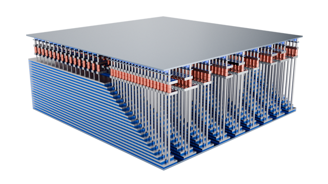
This set of technology, when applied to logic chips, may not have much practical use, but when applied to storage chips, it is truly a "nuclear weapon" because whether it is NAND or DRAM, the principles are not much different, both are transistor+capacitor structures with storage units and peripheral circuits.
So, based on crystal stack technology, two different units are separated into two total scores, processed independently, the most suitable process is selected, and then combined to achieve stronger performance and higher efficiency.
That's also why Changjiang Storage is based on applying Xtacking architecture to DRAM. I don't know how Samsung will handle it next.
