


Tight Capacity and a Scarcity of Chips: How Does CoWoS Create a Bottleneck for Global AI Chip Shipments?
According to reports from Taiwanese media citing supply chain sources, TSMC is preparing to raise prices for its CoWoS advanced packaging services, with an estimated increase of 10% to 20%. This rumor—which has yet to be officially addressed—stands in striking contrast to the attitude of downstream clients, who are reportedly willing to place orders as long as delivery schedules can be guaranteed. Amid the explosive demand for AI computing power, the packaging process—once considered the most inconspicuous back-end stage of the supply chain—has evolved into a critical bottleneck that dictates the shipment pace of AI chips.

Behind the Rumors of Price Hikes: Capacity Constraints Across the Entire Supply Chain
At the heart of these price-hike rumors is CoWoS—a 2.5D packaging technology that integrates logic chips with high-bandwidth memory (HBM) into a single package. It is widely used in high-end AI processors, such as those from NVIDIA. Demand for advanced packaging has expanded beyond AI GPUs to include server CPUs and custom ASICs, leading to a growing backlog of unfilled orders. Compounding this, the testing time for AI chips has increased significantly, further straining capacity in the assembly and testing sector.
This pressure is rippling throughout the entire supply chain. Industry insiders report that equipment lead times have stretched from the typical 3–6 months to 6–8 months. With clients prioritizing delivery schedules over cost negotiations, upstream suppliers of processing equipment and components are facing tight capacity, with little room for rapid expansion in the short term. A telling sign: while TSMC typically demands price reductions or added features from equipment suppliers during annual procurement cycles, this year the company has placed orders at original prices without negotiation—a clear indicator of robust demand.
The impetus for price increases stems from the fact that capacity cannot keep pace with demand. According to available data, TSMC’s monthly CoWoS capacity is set to grow from approximately 13,000–16,000 wafers in 2023 to about 70,000 by the end of 2025, with projections exceeding 130,000 by the end of 2026 and reaching roughly 200,000 by 2027. However, the demand curve is even steeper. Research from Morgan Stanley estimates global CoWoS demand at approximately 1.394 million wafers per year in 2026 and 2.694 million in 2027—with NVIDIA’s share expected to shift from about 60% to roughly 45% by 2027, as custom ASICs developed by cloud service providers emerge as a major new growth driver. UBS offers a similar outlook, projecting demand at 1.307 million wafers for 2026 and 2.475 million for 2027. While the specific figures vary, both sources reach the same conclusion: capacity expansion is failing to keep up with demand. According to a J.P. Morgan report, TSMC’s CoWoS production capacity stands at approximately 33,000 wafers per month as of the end of 2024. This is projected to reach 95,000 wafers per month by the end of 2026 and 112,000 wafers per month by the end of 2027; even by the end of 2026, the order fulfillment rate is expected to remain at only about 80%. Other industry reports estimate that by the end of 2026, TSMC’s internal monthly capacity will reach 120,000 to 140,000 wafers—or nearly 200,000 wafers when including outsourced capacity—with order backlogs extending into 2027.
Tight production capacity is directly driving up costs for downstream players. Should price hikes take effect, chipmakers such as NVIDIA and AMD will face higher costs. Apple’s iPhone and MacBook product lines—which have already seen price increases due to rising memory costs—may also come under renewed pressure. Other major clients, including Broadcom, Qualcomm, and MediaTek, are likewise among those affected.
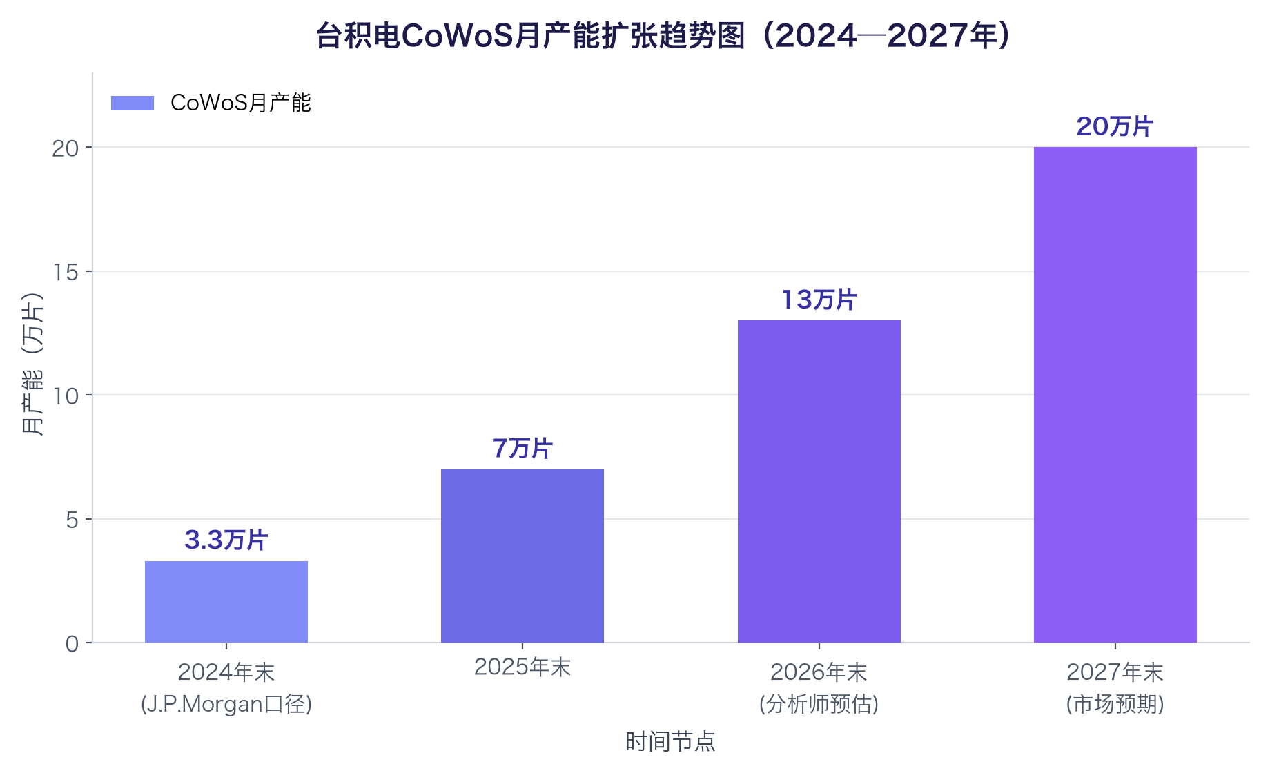
[Chart: Trend of TSMC’s Monthly CoWoS Production Capacity]
Chart Analysis: TSMC’s monthly CoWoS production capacity has expanded approximately fivefold over the past three years. However, given an estimated annualized demand exceeding 1.3 million units, a supply gap persists—the fundamental driver behind the current round of price increases.
TSMC’s Technological Depth: From CoWoS to CoPoS
To address shortages, TSMC is pursuing a dual-track strategy: capacity expansion combined with technological upgrades. During a recent earnings call, Chairman C.C. Wei stated that CoWoS remains the preferred solution for clients. TSMC is currently the only manufacturer capable of mass-producing packages at five times the reticle size (5x reticle) with excellent yields. Furthermore, the company is advancing 9x and 14x reticle solutions, as well as CoPoS technology, to accommodate larger-scale packaging requirements and reduce costs.
In terms of technical architecture, the CoWoS family has evolved into three variants: CoWoS-S, CoWoS-R, and CoWoS-L. The current mainstream 3.3x reticle-size configuration can accommodate eight HBM3 stacks; by 2027, this is expected to scale to an 8x reticle size, supporting 12 HBM4 stacks. A roadmap released by TSMC this April indicates that CoWoS has already advanced to a 5.5x reticle size. By 2028, the company plans to mass-produce a 14x reticle-size version, capable of integrating approximately 10 large compute chiplets and 20 HBM stacks. By 2029, TSMC intends to launch "SoW-X" (System-on-Wafer) technology—utilizing a 40x reticle-size footprint—with 3D-stacked SoIC (System-on-Integrated-Chips) technology also entering production that same year, alongside the A14 platform.
Perhaps even more promising is CoPoS—a "square-from-round" revolution in panel-level packaging. Traditional CoWoS relies on circular silicon interposers, which offer only about 65% area utilization of the circular wafer. CoPoS shifts to square panels, boosting utilization to 90%–95% and reducing unit costs by 20%–30%. A 510×515 mm panel offers 4.5 times the usable area of a 12-inch wafer, while a 600×600 mm panel can yield 5 to 6 times as many chips as a traditional wafer. TSMC has announced that its CoPoS (Chip-on-Panel-on-Substrate) technology entered pilot-line operation in June 2026. Mass production is slated for the AP7 facility in Chiayi, Taiwan, and a site in Arizona, USA, with a target timeline ranging from late 2028 to the first half of 2029. On the materials front, TSMC is collaborating with Japan’s Ibiden and Taiwan’s Innolux to develop glass-core substrates, and with Corning on specialized glass carriers.
The pace of capacity expansion is equally aggressive: it typically takes about three years for a new advanced packaging facility to progress from groundbreaking to reaching full capacity at its bottleneck stages, a process that includes facility construction, equipment installation, and subsequent calibration and validation. The production footprint includes the AP7 plant in Chiayi and the AP8 plant in Tainan, with the AP1 advanced packaging facility in the United States scheduled to begin production in 2028. To accelerate supply, TSMC is increasing its outsourcing, with ASE (Advanced Semiconductor Engineering) and its subsidiary SPIL (Siliconware Precision Industries) emerging as the primary beneficiaries.
A Global Race: Strategic Shifts Among Overseas Leaders and the Rise of Domestic Competitors
Advanced packaging has become the fastest-growing segment in the global semiconductor industry. According to a report by Yole Group, the global advanced packaging market reached $46 billion in 2024—a 19% year-on-year increase—and is projected to exceed $79.4 billion by 2030, with 2.5D/3D packaging experiencing the most rapid growth. DIGITIMES Research forecasts that the global market for AI chip packaging in data centers will grow from $5.6 billion in 2024 to $53.1 billion by 2030, representing a compound annual growth rate (CAGR) of approximately 45.5%. Meanwhile, SEMI predicts that global investment in AI infrastructure will reach $450 billion by 2026.
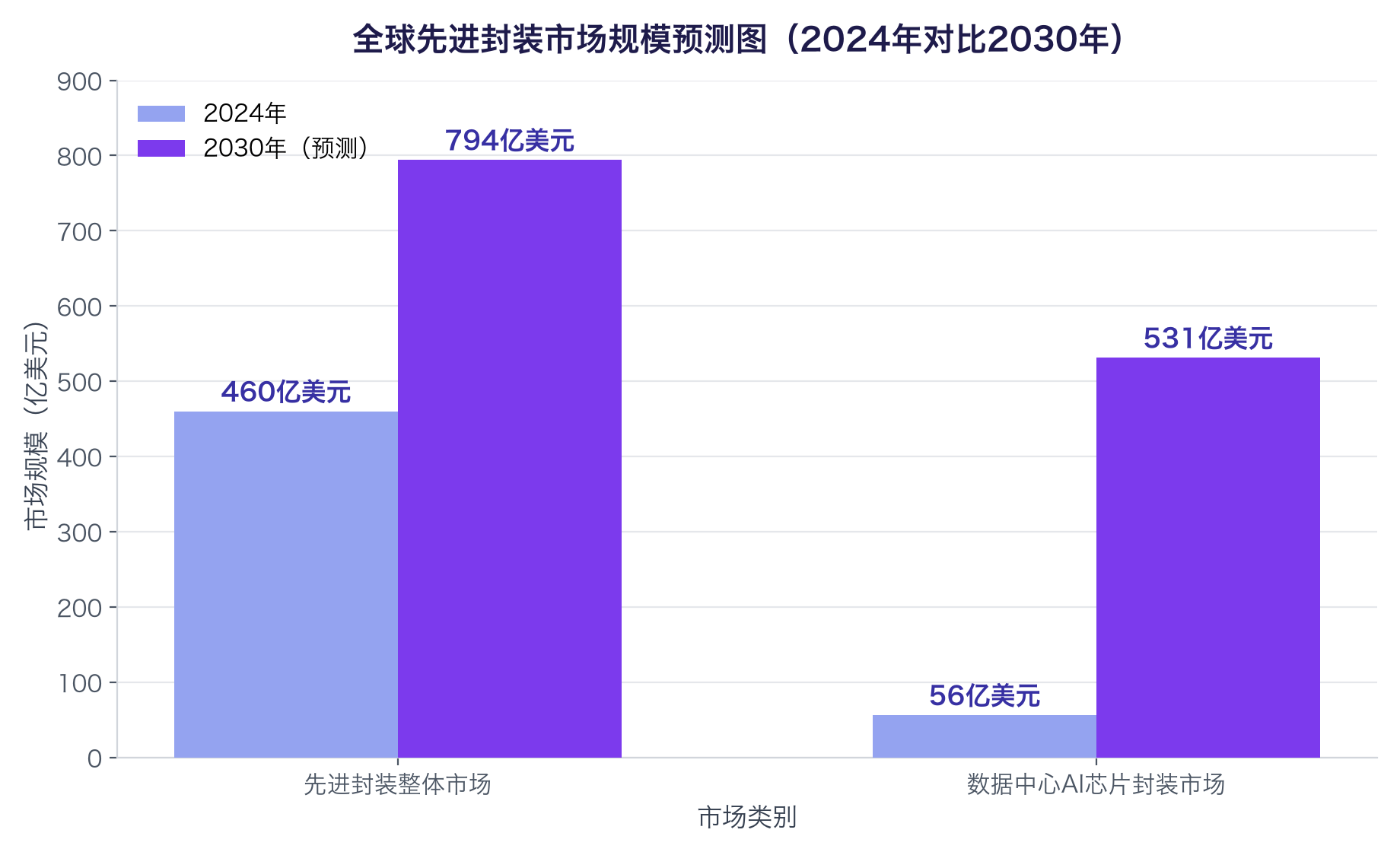
[Chart: Forecast of the Global Advanced Packaging Market]
Chart Analysis: The overall advanced packaging market and the market for AI chip packaging in data centers are projected to reach 1.7 times and 9.5 times their 2024 scale, respectively, by 2030. AI chip packaging serves as the primary driver of industry growth.
Among international players, Intel has adopted a "dual-track" strategy. Its EMIB-T solution offers a cost approximately 50% lower than that of CoWoS, with a yield rate of 98%. Intel also leads in the mass production of glass substrates, attracting clients such as MediaTek, Google, and Amazon. The company’s first-generation Foveros 3D stacking technology has already entered mass production and is utilized in Meteor Lake processors. In January of this year, Intel showcased a prototype integrating EMIB with a glass-core substrate (measuring 78×77 mm) and announced plans to retrofit its New Mexico facility into the world’s first mass-production site for glass substrates, with the goal of integrating 1 trillion transistors into a single package by 2030. Meanwhile, Samsung is pursuing a strategy combining its X-Cube 3D packaging with FOPLP (Fan-Out Panel-Level Packaging). In the OSAT (Outsourced Semiconductor Assembly and Test) sector, ASE (Advanced Semiconductor Engineering) is leveraging its FOCoS-Bridge technology to capture overflow orders from CoWoS; the company’s advanced packaging revenue is expected to grow by over $1 billion in 2026, building upon a projected $1.6 billion in 2025.
Players in mainland China are accelerating their efforts to catch up. JCET and Tongfu Microelectronics—both consistently ranked among the world’s top ten OSAT providers by revenue—are significantly increasing capital expenditures to develop localized production lines for CoWoS-like and HBM packaging. JCET’s XDFOI platform is spearheading the domestic alternative to 2.5D packaging, while SJ Semiconductor (SJ Semi) stands as one of only four manufacturers globally capable of mass-producing 2.5D packages. IDC also anticipates that as the OSAT industry ecosystem undergoes restructuring, the market share held by mainland China will continue to expand. According to industry reports, the domestic market for advanced packaging is projected to reach 170 billion yuan by 2026—a year-on-year increase of 25.9%—significantly outpacing the global growth rate. Local manufacturers have successfully achieved stable mass production for fan-out, 2.5D/3D, and TSV (Through-Silicon Via) processes, with overflow orders from overseas increasingly shifting toward domestic suppliers. Upstream supporting sectors are also gaining momentum: WOGE Optoelectronics’ TGV (Through-Glass Via) substrates can achieve a minimum via diameter of 3 microns with an aspect ratio of up to 150:1; its subsidiary, Hubei Tongge Micro, has already begun small-batch shipments from a production line with an annual capacity of 100,000 square meters. Meanwhile, the domestic market for 3D AOI (Automated Optical Inspection) equipment is expected to reach 5.38 billion yuan by 2026, growing at 27.2% year-on-year, as the trend toward domestic substitution accelerates.
Trend Analysis: Shortages May Persist Until 2028; Glass Substrates Emerge as a Decisive Factor
The current cycle of shortages may last longer than the market anticipates. While investment banks previously projected that the CoWoS supply gap would close by the end of 2027, industry research suggests that glass substrates will likely require another 2 to 3 years before reaching full-scale mass production, meaning CoWoS shortages could persist at least until 2028. Although there were concerns that TSMC might leverage the supply crunch to push price hikes beyond 30%, recent discussions indicate a preference for building long-term partnerships with clients rather than pursuing short-term, aggressive price surges. Instead, the company aims to drive profitability through capacity expansion and improved yields; the estimated price increases of 10% to 20% reflect this "balance between volume and price" strategy.
In terms of technology, glass substrates combined with TGV (Through-Glass Via) are widely regarded as the future of packaging substrates. This approach offers a 16% improvement in package warpage, a 19% reduction in the effective coefficient of thermal expansion (CTE), a 27% decrease in electrical resistance, and a 42% reduction in inductance—effectively addressing the dual challenges of warpage in large-format packages and the high costs associated with silicon interposers. Co-Packaged Optics (CPO) represents another critical frontier. TSMC’s Compact Universal Photonic Engine (COUPE) is slated for mass production by 2026, offering a two-fold improvement in energy efficiency and a 90% reduction in latency compared to traditional pluggable solutions.
The current wave of price increases is, at its core, a revaluation of industrial value driven by the structural expansion of demand for AI computing power. Packaging has shifted from a "back-end supporting role" to a "front-end bottleneck," now commanding a strategic importance on par with wafer fabrication. For downstream chipmakers, a 10% to 20% rise in costs secures scarce production capacity—a trade-off that remains highly cost-effective in a market defined by shortages. For the supply chain in mainland China, the spillover of overseas orders, combined with emerging opportunities in areas like glass substrates and CPO, presents a rare chance to catch up. As advanced process nodes approach their physical limits, the synergistic optimization of packaging and fabrication will collectively define the next upper bound for AI chip performance.
