


Samsung HBM is handed over to TSMC for the first time, with custom controllers integrated into the underlying chip
Recently, the Seoul Economic Daily reported that Samsung Electronics has decided to use TSMC's 3-nanometer process to produce substrate die for Nvidia's next-generation customized HBM.
Samsung's approach to HBM has always been filled with the pride of a conglomerate. From DRAM core die to substrate die, and then to packaging testing, all are completed in a closed loop by our own production line.
The HBM4, which was mass-produced in February this year, is the pinnacle of this route. The core die uses the sixth generation 1c DRAM process, and the substrate die uses the 4-nanometer logic process of our own foundry department. The customer received a thorough Samsung product.
This turnkey model was once ridiculed by the outside world as a complex system, but Samsung itself sees it as a moat against the professional division of labor camp.
Nvidia has no interest in appreciating this moat, and the changes were pushed to the extreme in August 2026. Nvidia released a customized storage architecture NVHBM, which moved the storage controller originally located inside the XPU into the HBM base and equipped it with a self-developed physical layer interface.
According to official sources, this design can reduce the area of PHY and auxiliary circuits by up to 67%, freeing up up up up to 25% of the area for computing chips to stack computing power circuits. The single stack bandwidth can be increased by up to 30% compared to the standard HBM4E, and power consumption can be reduced by up to 15%.
Subsequently, it issued a unified requirement to three suppliers, Samsung, SK Hynix, and Micron, stating that all substrate die must use TSMC's 3-nanometer process, and all core die must use 1c DRAM process.
According to industry sources, Amazon Annapurna Lab has decided to design the next generation Trainium4 accelerator using NVLink Fusion and NVHBM.
The number of layers determines the upper limit of capacity, while the base determines the lower limit of performance. This chip has become the winner of the entire product line.
The lethality of this requirement lies in its denial of Samsung's sovereignty, which Samsung's Device Solutions Division has chosen to accept after internal evaluation. The vertically integrated fortress that has persisted for more than 20 years has opened its doors to competitors for the first time in the manufacturing process.
What Nvidia wants is not stronger memory, but a more obedient supply chain
On the surface, NVHBM is a technological upgrade. Compared to the standard HBM4E, NVHBM can increase memory bandwidth by up to 30%, reduce power consumption by up to 15%, and significantly reduce the physical layer footprint of the chip.
Moving the controller from the computing chip to the base die also frees up valuable chip area for the GPU, which can accommodate more computing units.
Underneath the technological dividend lies a colder calculation. Previously, the three storage factories each developed their own design and manufacturing processes for the substrate die, and Nvidia had to go through the compatibility and performance verification process again for every supplier it imported.
In the rhythm of annual generation of AI chips, after unifying the 3-nanometer substrate process, the products of the three companies can be seamlessly exchanged on the Nvidia platform, saving verification resources and shortening the import cycle.
Nvidia did not choose one of the three suppliers for exclusive favor, but flattened all the bottom layers of the three suppliers, allowing them to compete for the real effort of DRAM stacking on the same logic foundation produced by TSMC. The substitutability between suppliers was institutionalized, and pricing and discourse power were concentrated towards buyers.
TSMC didn't do anything, just stood there and became the biggest hardware beneficiary of this standardization movement, capturing the most technologically advanced layer of logic in HBM.
Transferring a 3-nanometer substrate is a face for face transaction
Samsung's concessions are not without cost, and the substrate bare chip is precisely the fattest piece of meat in its OEM business at present. According to industry sources, about 50% to 60% of Samsung's 4-nanometer production line is producing HBM4 substrate wafers, and the Pingze factory's monthly output of tens of thousands of wafers supports the utilization rate of the foundry department.
Thanks to the high volume of HBM4, Kiwoom Securities estimates that the combined operating loss of Samsung's wafer foundry and system LSI businesses in 2026 will narrow by 41.8% year-on-year, from KRW 6.74 trillion to KRW 3.92 trillion.
In July, Samsung even raised the price of new orders for 4 nanometers, with some nodes experiencing a 10% to 15% increase. Giving the NVHBM substrate bare chip to TSMC is equivalent to cutting open another wound that is currently stopping bleeding.
On the other side of the account, it is equally clear that in the second quarter of 2026, Samsung's market share in the global HBM market has rebounded to 33%, narrowing the gap with SK Hynix's 50% market share to 17 percentage points.
SK Hynix has outsourced the substrate die to TSMC since HBM4, and Micron announced early that HBM4E's logic substrate will fully cooperate with TSMC.
On the customized HBM table, Samsung is the only player still holding a fully self-produced shelf, which is becoming a burden. The customer wants customization, and Samsung's fully integrated solution cannot cover all specification requirements.
Samsung's shrewdness lies in its discretion, maintaining full in-house production for standard HBM and customized products for other customers such as AMD.
The core DRAM die and stack packaging, which truly determine yield and capacity, have not been compromised even by a millimeter. It also holds the feasibility verification of producing NVHBM substrates on its own production line, and the 2-nanometer process is listed as an alternative to prevent TSMC's production capacity from peaking.
Letting go is the manufacturing rights of a layer of bare chips, while guarding the entrance ticket to Nvidia's supply chain and the hidden door that can be retrieved at any time.
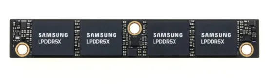
In the second half of HBM, the winner moved from the stacking layer to the logical base
The most profound impact of this collaboration is that it announced the migration of the HBM competitive coordinate system. Before HBM4, DRAM technology was sufficient for substrate bare chips, and the competition among storage factories focused on stacking layers, TSV yield, and packaging routes.
HBM4 doubles the I/O width, pushing the base die towards advanced logic technology. Customized HBM goes further, and customers' memory controllers, interface logic, and even near memory computing modules must be written into this layer of base. Memory is becoming a system component that system manufacturers personally participate in defining.
As the coordinate system changes, the technological barriers for DRAM stacking remain high, and incremental value is accelerating towards customized logic in the substrate die.
Nvidia took away the definition rights with buyer power, TSMC took away the manufacturing rights with process capability, leaving the DRAM industry and packaging to the storage plant.
The center of the profit pool is moving, and the three storage powerhouses are evolving towards high value-added assembly integrators. Samsung's response was the most honest among the three, as it made concessions while stuffing the design talent it had poached from its system LSI department into its storage business unit, preparing to personally write designs on the customer's base die.
Ending
The memory has grown logic, and the boundaries of computation have become loose. Samsung handed over the manufacturing rights for a base chip and received the admission ticket for the AI storage card table.
