


MRAM domestic industrial chain is being connected
There are only a few companies in the world that can achieve mass production of MRAM. For a long time, this track has been dominated by a few top players: Everspin is the only publicly traded company in the world with MRAM as its main business; Samsung and TSMC will integrate embedded MRAM into advanced logic processes; NXP applies MRAM to automotive grade MCUs.
In this small circle, the presence of domestic manufacturers is rapidly increasing: Chituo Technology's MRAM products have achieved mass production and entered the industrial and automotive regulatory fields; Commercial shipment of STTMRAM from Siprion in Shanghai has been completed; The SOTMRAM chip developed by Zhizhen Storage has been validated in drone flight control. Behind the rise of domestic manufacturers is the gradual formation of a complete industrial chain.
Not only in the terminal application stage, but also in the upstream critical materials, core equipment and other weak links, breakthroughs are being achieved one by one.
01 Material: The final addition is a layer of magnesium oxide
The core storage unit of MRAM is a magnetic tunnel junction (MTJ), which is composed of multiple layers of metal and insulating thin films with a thickness of less than ten nanometers, and relies on the magnetic moment direction of the magnetic layer to complete data storage. To prepare this multi-layer film, a series of high-purity sputtering targets are required, including cobalt iron boron magnetic targets, platinum manganese antiferromagnetic targets, ruthenium and other metal spacer targets, as well as magnesium oxide targets that serve as insulation barriers. With the help of high-precision sputtering technology, ultra-high purity magnesium oxide can be deposited into ultra-thin single crystal films with a thickness of 12 nanometers, forming a uniform and dense insulation barrier structure. The regular lattice structure can generate stable spin filtering effect, screen electrons with specific spin states to complete quantum tunneling, provide basic structural support for chip magnetoresistance conversion and data reading and writing, and is a key carrier for realizing MRAM storage function.
In August of this year, Suzhou Zhicai Technology announced the success of its independently developed 6-inch MRAM MgO target material. This product is semi transparent, with a purity of 4N, a density of>99.8%, and key indicators such as grain uniformity that have reached international advanced levels (the density of similar mainstream target materials in Japan is>99.7%). This means that the mainstream domestic MRAM chip manufacturers and research institutions that were previously affected by international interference now have the option to independently control the supply of domestic core materials.
Magnesium oxide targets are used for the insulation barrier layer of MTJ, and the quality of the sputtered thin film directly determines the tunneling magnetoresistance ratio and yield of the device, which has long relied on imports. Therefore, the industry has set extremely high technical thresholds for indicators such as purity, density, and grain uniformity of the target material. Prior to this, the remaining metal magnetic target materials required for MTJ multilayer films have been basically localized and self-sufficient, with magnesium oxide being the last shortcoming.
In addition, domestic manufacturers such as Yan Yijin and Henan Dong Microelectronics Materials have entered the supply chain of spin chip target materials. It is reported that Dong Microelectronics' MRAM series target materials have the highest market share in China, with leading suppliers of cobalt iron boron targets, magnesium oxide targets, and other bulk supplies. Among them, cobalt iron boron targets are exclusively mass-produced domestically.
The true significance of material localization lies not in individual target materials, but in supply safety. Most of the main research and development institutions of MRAM are facing the dual constraints of overseas key materials, and the risk of target material supply interruption has always been hanging on the production line. Now that all functional layer materials of magnetic tunnel junctions can be found in domestic suppliers, this risk can be truly eliminated.
02 Equipment: MRAM now has dedicated process equipment
Pushing down one layer of material is the equipment that carves these thin films into devices. The milling of magnetic tunnel junctions is the most crucial process step in the fabrication of MRAM devices. On the one hand, the magnetic tunnel junction is composed of over 20 sub nanometer thick metal functional film layers (involving platinum, iron, cobalt, manganese and other metal materials) and oxide dielectric layers (magnesium oxide). The quality of film formation in each layer and the physical and chemical bonds formed at the interface between the film layers are closely related to the performance of the memory device. If traditional plasma etching is used, the metal etching residue cannot form volatile substances that are pumped away by the vacuum pump group, inevitably causing the residue to accumulate on the side walls of adjacent magnetic tunnel junctions and equipment reaction chambers, resulting in contamination and short circuits, thereby causing device performance failure and reduced production yield. Especially with the advancement of logic circuit technology, device sizes continue to shrink, and compatible magnetic tunnel junction sizes also become smaller and denser, leading to increasingly severe residue accumulation problems. On the other hand, after completing the etching of the magnetic tunnel junction, if the magnetic tunnel junction is exposed to the atmospheric environment, it will react with water vapor in the atmosphere, causing device failure.
Jiangsu Leuven Instruments is a representative domestic enterprise in this field. The ion beam shaping equipment developed by it integrates one ion beam shaping (IBS) chamber, two ICP etching chambers, and one PEVCD chamber on the same vacuum transfer platform. On the one hand, the use of IBS and ICP etching chambers in conjunction to complete the milling of magnetic tunnel junctions can effectively solve the above-mentioned process problems such as metal sidewall contamination, making large-scale production of emerging memory devices such as MRAM possible. Compared to the current international leading manufacturer Panlin Semiconductor, which only uses ion beam shaping technology for milling magnetic tunnel junctions, the synergistic etching method of ion beam shaping and ICP etching has a faster etching rate and higher yield. On the other hand, the ion beam shaping equipment integrates one PECVD process chamber, which can achieve the deposition of a passivation layer on the magnetic tunnel junction in the vacuum environment inside the equipment after etching is completed, effectively isolating the air and avoiding device failure. In addition, the ion beam shaping equipment is further integrated with an ICP etching process chamber, which can complete the necessary hard mask layer etching before the magnetic tunnel junction etching, further improving the integration of the equipment and enhancing mass production efficiency.
LMEC-200, the first generation emerging memory process equipment of Leuven Instruments, won the order of Taiwan, China Industrial Research Institute from international manufacturers in 2018; The upgraded 12 inch LMEC-300 has been delivered to customers and achieved acceptance and sales. It was selected for the first major equipment list in Jiangsu Province in 2022. In June of this year, Leuven Instruments' IPO on the Science and Technology Innovation Board was accepted, with plans to raise 2.5 billion yuan.
In addition to the front-end process equipment, the back-end testing equipment was also a shortcoming that was easily overlooked in the industry. The testing of magnetic chips requires synchronous completion of electrical reading and writing and failure bitmap acquisition in a controllable magnetic field and wide temperature environment, which cannot be done by general-purpose testing machines. The spin chip reliability testing equipment developed by Qingdao Zhizhen Precision Instrument can provide a uniform magnetic field of up to 2000 Oe and a temperature environment of -55 ℃ to 170 ℃. It has entered the SOT-MRAM magnetic immunity research of research teams such as Beihang University; Its wafer level magneto-optical Kerr measurement instrument, tunneling magnetoresistance ratio measurement instrument and other products cover multiple nodes from research and development characterization to mass production testing.
03 Manufacturing: Achieving closed-loop MRAM mass production
After the equipment and materials are in place, the production line becomes the link that determines the quality of the industry.
Chituo Technology has its own 12 inch MRAM production line, forming three mass production platforms of 90nm, 40nm, and 28nm. It can provide independent products and embedded IP customization, and is the only manufacturer in China that can provide mass production MRAM products. The team independently develops and masters the key technologies of the entire chain of third-generation MRAM (STT-MRAM) chips from design, components, process manufacturing, testing and evaluation to application development. The products cover a capacity of 256kb~64Mb and are widely used in fields such as intelligent IoT, industrial automation, enterprise storage, identity authentication, artificial intelligence, and commercial aerospace.
However, it should be noted that the embedded MRAM process window for advanced manufacturing is still overseas. Hanxu Technology's 8nm eMRAM chip is based on Samsung's technology, and TSMC is expected to complete the production preparation of 5nm MRAM by 2027. The domestic manufacturing process has already closed in the mature manufacturing process, and there is still a significant gap compared to TSMC and Samsung in advanced eMRAM.
04 Device: Three routes advancing simultaneously
Above the production line, there is a division of routes at the device level. The current overall pattern of domestic MRAM can be summarized as follows: "STTMRAM has achieved industrialization, SOTMRAM has made breakthroughs in cutting-edge technology, and MRAM storage and computing integration has achieved global integration".
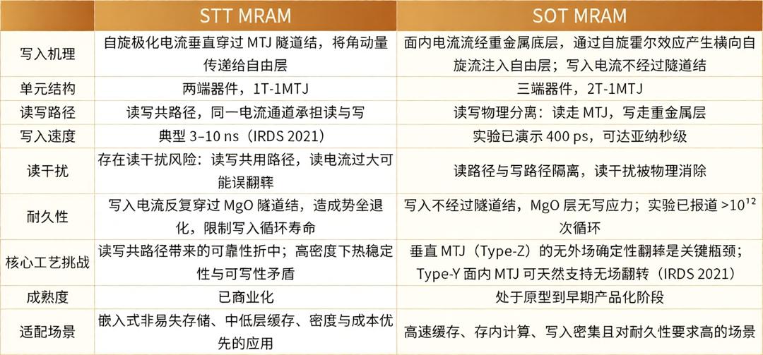
The commercialization progress of STTMRAM is relatively fast. Chituo Technology has built a product matrix ranging from Kb to 100Mb, and Shanghai Siporin has already achieved commercial shipment. Looking globally, Everspin's latest UNISYST MRAM product has a density of 128Mb2Gb and a read bandwidth of 400MB/s, targeting the approximately $3 billion standalone NOR Flash replacement market. In the independent MRAM track, the technology gap between domestic enterprises and international giants is continuously narrowing.
SOT line represents the direction of next-generation technology. SOT-MRAM uses spin orbit torque to drive magnetic moment flipping, resulting in faster read and write speeds and higher durability, but the device structure and process are more complex. The 256Kb SOT-MRAM chip from Zhizhen Storage has completed commercial verification in drone flight control; Chituo Technology has innovatively proposed a channel less (CHL) device architecture, which integrates the design of tunnel junctions and track layers. The device can be prepared in one etching process, and the bottom contact electrode (BE) can be etched during etching, increasing the device yield to over 99.9%; The National Key Laboratory of Spin Chip and Technology has released the world's first fully functional third-generation MRAM chip with a single chip capacity of 4 Mb - SOT-MRAM chip, which is also the world's first vertically magnetized SOT-MRAM chip with Mb capacity.
The storage and computing integrated line is betting on AI. The MRAM storage and computing integrated chip embeds matrix multiplication operations inside the storage unit, eliminating the huge energy consumption caused by repeated data transfer between storage and computing units in traditional architectures. Previously, the Key Laboratory of Information Storage Systems at Huazhong University of Science and Technology released the "Yujiashan No.1", which was the world's largest MRAM storage and computing integrated chip at that time. It used a national production process and consumed only one thousandth of the power of traditional chips. In June of this year, the research and development of the "Yujiashan No.2" chip entered a critical period. The "Yujiashan No.2" chip will be iteratively upgraded based on the "Yujiashan No.1" technology, further improving computing power and energy efficiency. The team from Southern University of Science and Technology has successfully designed and verified a 64kb non-volatile digital memory computing integrated chip using 40nm CMOS and STT-MRAM processes. The chip achieves multiplication of single bit input and storage weights in STT-MRAM bit cells and directly outputs digital results; The 8nm eMRAM AI chip from Cold Sequence Technology combines embedded storage with storage computing architecture, supporting end-to-end operation of 2 billion parameter level large models.
The value of the device ultimately needs to be released through practical scenarios. MRAM has characteristics such as non-volatile, nanosecond level writing, trillions of erasures, wide temperature range, and radiation resistance. It will not be the first to enter the consumer storage market, but will prioritize establishing market advantages in automotive and industrial scenarios with strict reliability requirements; Edge AI is a newly opened incremental track. The inference of end side large models is limited by power consumption and space, and the size of eMRAM cells is much smaller than SRAM and does not require refreshing, providing new storage options for end side devices.
05 Conclusion
After the various links in the industrial chain are gradually connected, the construction of industrial ecological synergy is also accelerating. In December 2025, the first spin chip and technology seminar was held in Hangzhou, and the spin chip industry innovation alliance was unveiled. Domestic MRAM has passed the stage of "individual breakthrough" and has begun to have industrial organization and technical specifications. For industries with heavy assets, long cycles, and strong collaboration such as new storage, the value of alliances and standards is no less than a single technological breakthrough. They determine whether enterprises on the chain can collaborate in the same language.
Between 2025 and 2026, domestic MRAM will cross the threshold in five aspects: materials, equipment, manufacturing, design, and application. The localization of target materials and etching machines has reduced the cost of building production lines, and the implementation of production lines has increased the iteration speed of design teams. The maturity of devices has in turn supported alliances and standards. But the shortcomings are still clear: the process window for advanced process eMRAM is still in the hands of TSMC and Samsung. But the significance of connecting the industrial chain lies here. The competition that follows is no longer a race between individual links and international standards, but a comprehensive attack on the generation gap through a complete chain.
