


Board-Level Packaging: Key Design Points for High Voltage Differential Products
With the rapid growth in demand for consumer power supplies, industrial control, and automotive power chips, board-level packaging has become an important development direction for advanced packaging due to its features of large-area carrier boards, high integration, and high interconnection efficiency. Unlike traditional wafer-level packaging, board-level packaging completes multi-chip integration and rewiring manufacturing on large-size substrates, offering greater design freedom and cost advantages, providing a new technical path for mass production of high-voltage power chips.
However, high-voltage conditions impose strict requirements on insulation withstand voltage and leakage control, making it impossible to directly follow conventional low-density board-level packaging design rules. A dedicated design system for high-voltage products must be established. For this technical direction, leading packaging and testing companies such as JCET and Tongfu Microelectronics, as well as several innovative companies focused on advanced packaging, have all actively laid out their strategies.
The packaging evaluation of high differential pressure products primarily focuses on the actual operating conditions of the end-user terminal. In terms of insulation safety, priority is given to selecting insulating dielectric layers that are high-temperature resistant, have high breakdown strength, and have low ion precipitation, to suppress ion migration and leakage risks at high temperatures; In layout design, strict line spacing rules are followed for voltage difference matching, with sufficient safety distances reserved between conductors at different potentials to avoid creep on the dielectric surface. In addition, special attention must be paid to controlling conductor edge fillet treatment and the integrity of dielectric coverage to avoid electric field concentration caused by sharp corners; At the same time, a voltage withstand design margin is reserved in combination with the temperature and humidity conditions of the application environment, ensuring insulation stability throughout the product's entire lifecycle.
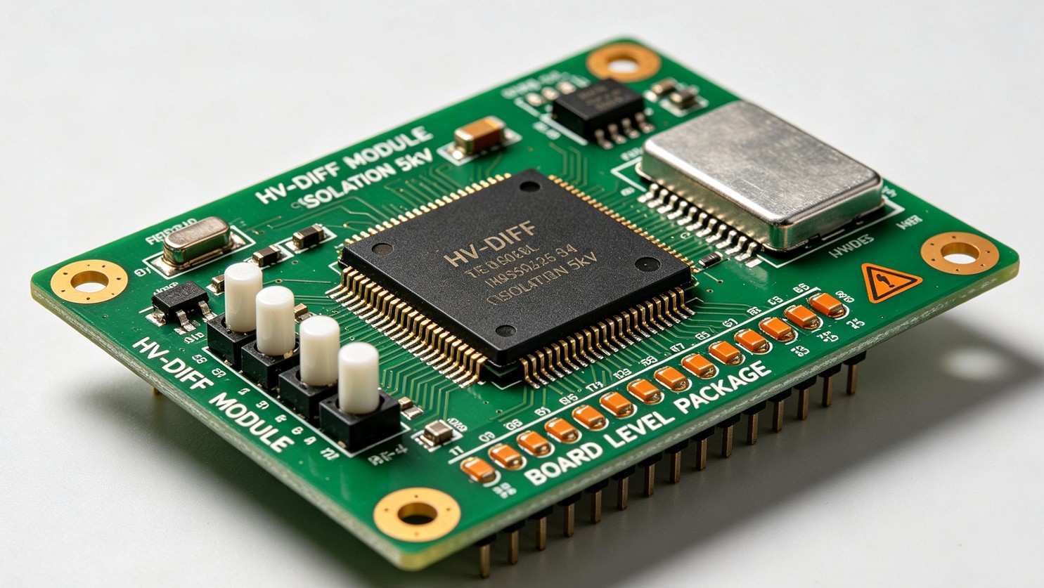
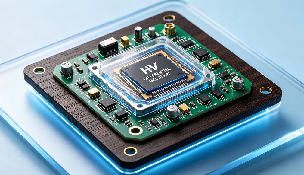
There are multiple common industry challenges in high-pressure differential board-level packaging design. First, stress control on large slab surfaces is difficult, easily causing cracking and delamination of the insulating medium; Second, the electric field concentration effect is significant, and adjacent layouts easily cause creeping and breakdown; Third, process uniformity is highly challenging, as fluctuations in media thickness weaken breakdown resistance. Conventional board-level design rules cannot cover insulation, creeez-in, and ion migration requirements in high-voltage scenarios; if applied directly, reliability verification is prone to failure.
To address these pain points, the domestic packaging and testing industry chain is making technological breakthroughs from different dimensions. On one hand, leading OSAT vendors such as JCET and Tongfu Microelectronics leverage their full-process advantages to accelerate system-in-package technology iteration; On the other hand, in the board-level packaging niche, many innovative companies are also approaching from the design side, exploring solutions better suited to high-voltage scenarios. Among them, as a leading domestic company in the board-level fan-out packaging field, Jiangsu Pangu Semiconductor Technology Co., Ltd. (hereinafter referred to as "Pangu Semiconductor") adopts a system-level approach of "design and simulation pre-loading" to build a board-level packaging design solution for high dropout products.
At the design level, the scheme establishes dedicated design specifications for high dropouts: defined graded creepage and electrical gap standards based on application voltage and usage environment, enforcing isolation of high and low voltage zones; Using electric field simulation tools to pre-simulate the distribution of electric fields within the layout, optimize traces and pad structures, and reduce the concentration effect of the cutting-edge electric field; At the same time, combined with stress simulation collaborative evaluation, chip positions are reasonably arranged to reduce warpage stress damage to the insulating medium. Additionally, Pangu Semiconductor conducts a special high differential pressure differential assessment during the manufacturability design stage, making dielectric material selection, line spacing, shielding structure, and edge protection mandatory inspection items, intercepting insulation design defects before plate placement and avoiding voltage failure risks at the source.
The design corresponding to this solution also features several unique features of high differential pressure:
High-voltage differential pads and traces are arranged in a zoned layout, with sufficient creepage distance and electrical clearance reserved in between, and adjacent conductors maintained at safe distances to avoid staggered arrangement;
All metal pads and trace corners use a rounded design to reduce the concentrated electric field effect at the tip;
Maintain sufficient high-voltage differential insulation margins at the edge of the plastic encapsulation to prevent creepage along the surface of the plastic encapsulated body.
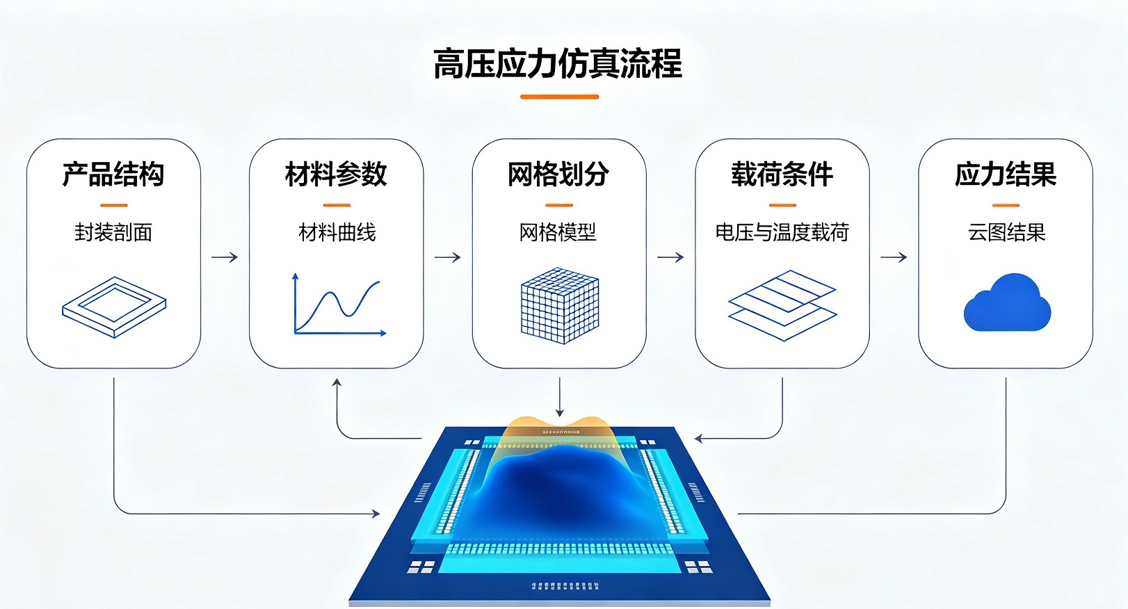
From an industrial deployment perspective, Pangu Semiconductor's solution advances joint multiphysics simulation evaluation into the design phase, allowing integration density to be maintained while ensuring high-voltage safety. Relying on comprehensive high-voltage board-level packaging design specifications, customized development can be carried out for different pressure differential levels and automotive/industrial application scenarios; Through full-chain collaboration between design and process, it helps customers reduce R&D trial and error costs and shorten product implementation cycles. The solution strikes a balance between high-voltage insulation safety, integration density, and mass production yield, providing technical support for the industrialization of board-level packaging for domestically produced high-voltage power chips.
As power semiconductors continue to upgrade toward high integration and reliability, the high-voltage adaptability of board-level packaging will become the core competitive edge in this segment. Continuous exploration by local packaging and testing manufacturers across different dimensions such as process, design, and materials will jointly drive steady upgrades in domestic power packaging technology.
