


According to reports, Samsung Electronics plans to complete the development of the advanced packaging technology '3D Cube-H' early next year.
According to a report by ZDNET Korea, Samsung Electronics has formulated plans to complete the development of its advanced packaging technology "3D Cube-H" early next year.
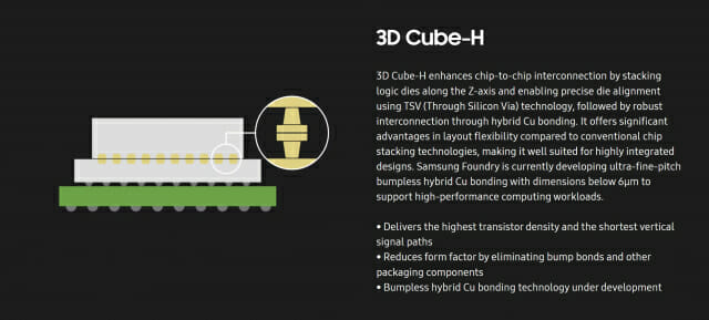
According to reports, 3D Cube is an advanced packaging technology that vertically stacks multiple chips. Compared to traditional chip horizontal arrangement structures, 3D Cube can integrate more transistors within the same area. Samsung Electronics previously developed the hot-bonding (TC Bonding) 3D Cube-T and is currently developing hybrid bonding (note: Hybrid Bonding) 3D Cube-H.
The main application direction of 3D Cube-H is ultra-high-performance AI chips. If Samsung Electronics successfully develops this technology, its foundry business is expected to secure major client orders.
An industry insider familiar with the matter said: "Samsung Electronics has long been actively developing hybrid bonding technology for 3D system (logic) chips. The company plans to complete its first design kit early next year, after which it will begin evaluating potential customers. "
Samsung Electronics has been developing 3D Cube-H with a terminal pitch of about 6 μm. For comparison, chips currently using traditional TC bonding technology have terminal pitches of at least about 25 μm, while 3D Cube-H has much smaller pitches.
Another semiconductor industry insider said: "Using hybrid bonding technology can greatly increase the connection density between chips while reducing power consumption per bit. In terms of heat dissipation, this technology also has advantages over TC bonding ”
