


World's first! Infineon achieves the world's first 300 mm silicon carbide wafer functional power device at its Villach, Austria factory
Recently, Infineon Technologies AG announced that it has successfully processed 300 mm silicon carbide (SiC) wafers into functional power devices at its Bellach plant in Austria, becoming the world's first company to achieve this milestone in a large-scale semiconductor wafer fab environment. At the electronica 2026 exhibition opening in Munich on November 10, Infineon also showcased its first fully processed 300 mm silicon carbide wafer to the public.
300 mm single wafer chip yields up to 2.3 times that of 200 mm chips
silicon carbide is a key semiconductor material for achieving efficient power conversion: with its excellent material properties, it achieves lower power loss and higher power density, and can operate efficiently in high-voltage and high-temperature environments. It is widely used in traction inverters, onboard chargers, electric vehicle charging stations, large-scale energy storage systems, industrial transmission devices, and uninterruptible power supplies—AI data centers are also seeing growing demand for silicon carbide, with applications further expanding to solid-state transformers, circuit breakers, and power supply units.
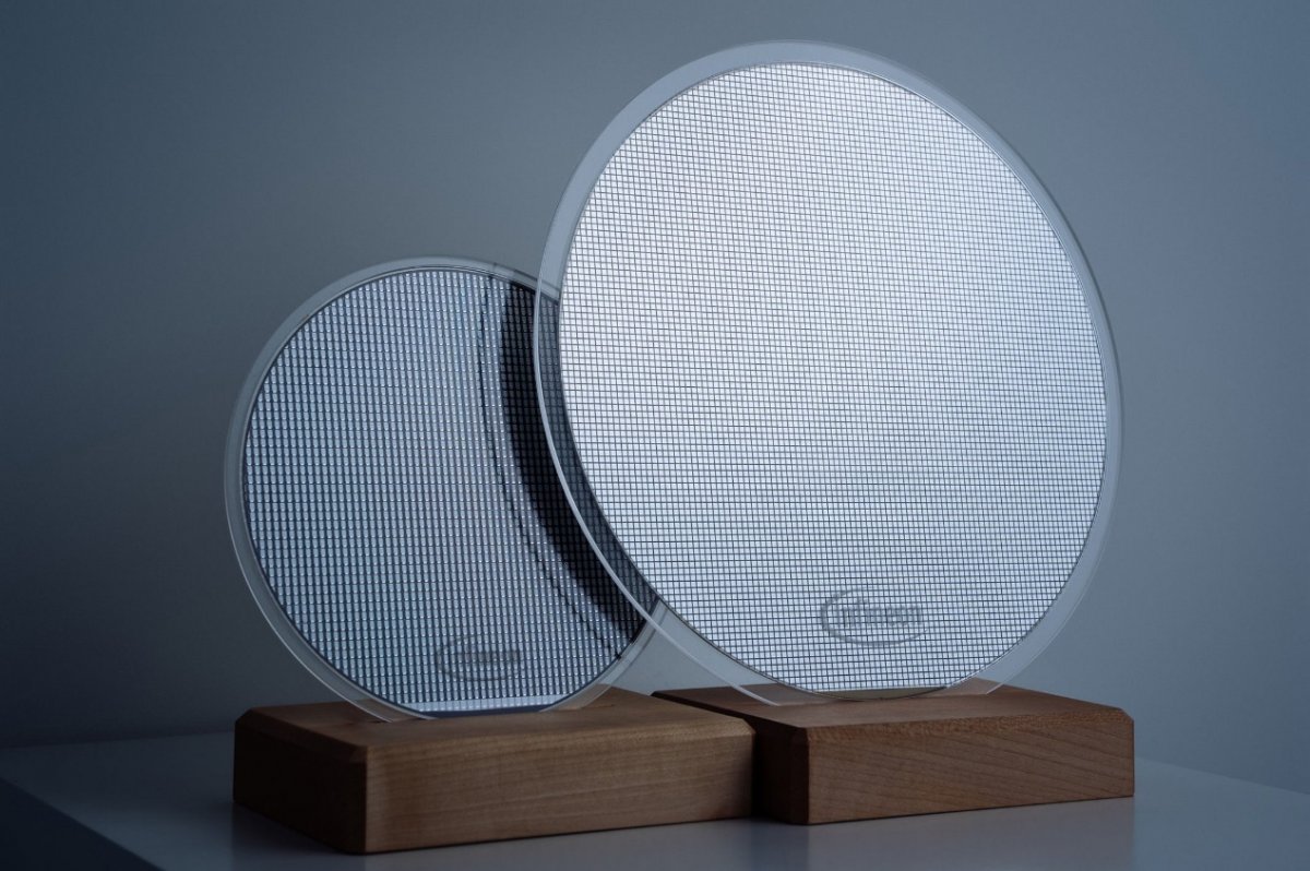
300 mm silicon carbide wafer: Compared to 200 mm wafers, 300 mm wafers can produce 2.3 times more chips per single wafer than 200
mm wafers
Compared to 200 mm wafers, 300 mm wafer chip production technology is more advanced and efficiency is greatly improved: thanks to the larger wafer diameter, the number of chips produced per wafer can reach 2.3 times that of 200 mm wafers. However, moving 300 mm silicon carbide from the lab to large-scale production is not easy—Infineon CEO Jochen Hanebeck specifically mentioned in his congratulatory speech that it is the team's "relentless efforts that have made significant progress in advancing 300 mm silicon carbide technology from the lab to large-scale production."
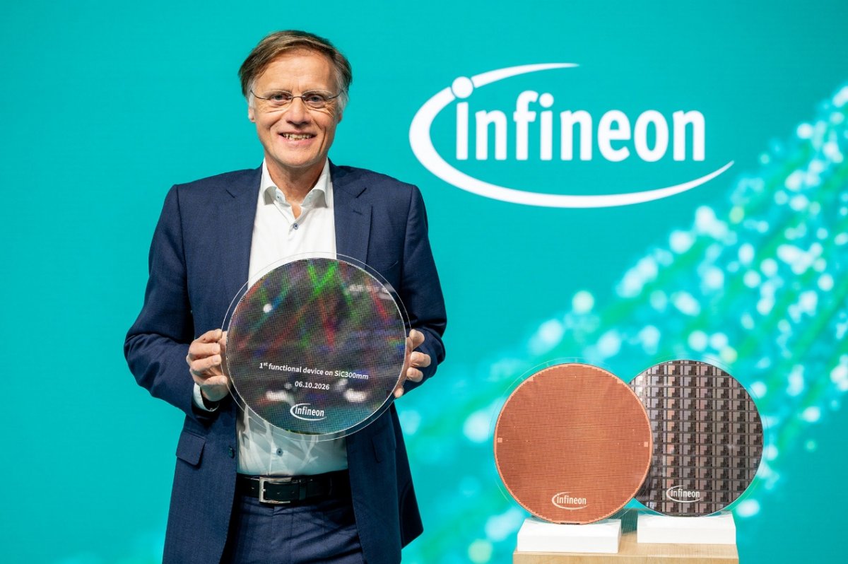
Jochen Hanebeck, CEO of Infineon Technology AG, poses with 300 mm silicon carbide wafers, 300 mm ultra-thin silicon wafers, and 300 mm gallium nitride
wafers
How did Infineon break through? Using existing silicon equipment to produce silicon carbide also overcomes the challenge of "cold cutting
"
The key to this breakthrough is that this achievement is realized using Infineon's existing silicon manufacturing equipment—meaning there is no need to build a new production line from scratch, providing a practical path for the feasibility of the 300 mm silicon carbide process. Meanwhile, Infineon successfully validated the feasibility of cold split technology for 300 mm silicon carbide wafers at its Dresden plant in Germany: compared to traditional wire saw cutting processes, cold splitting can separate wafers from silicon carbide ingots, reducing material loss and significantly shortening processing time, allowing for more wafers from the same ingot with lower capital expenditure.
Infineon stated that it will work closely with customers and partners to plan the 300 mm silicon carbide technology roadmap and ramp-up pace, while continuously advancing the existing 200 mm silicon carbide manufacturing roadmap—these two routes are running in parallel, aiming to provide advanced silicon carbide power technology that is cost-effective and stable in supply.
With this, Infineon has mastered all three 300 mm wafer technologies for semiconductor-related materials: silicon, silicon carbide, and gallium nitride. On October 27, 2026, Infineon just announced an investment of about 1.1 billion euros to build a large-scale mass production base in Villach using 300 mm wafer technology to produce gallium nitride (GaN) power semiconductors; This achievement in the silicon carbide field extends this model to a second wide bandgap material.
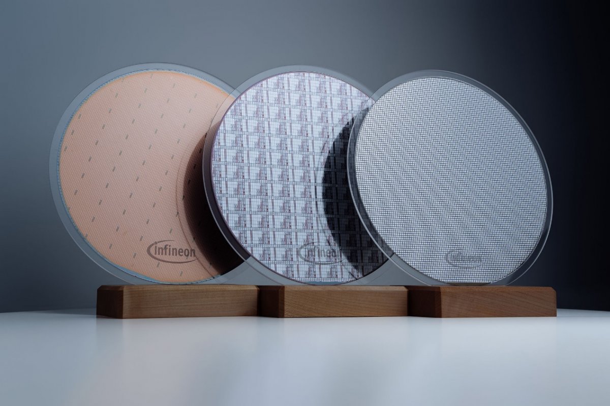
Infineon now masters 300 mm wafer technology for all three materials: silicon, silicon carbide, and gallium nitride
Fiscal Year 2026 closes to a record high, data center power supplies are highly anticipated
Behind these technological milestones lies a strong operational foundation. Infineon's financial report for fiscal year 2026 (ending September 30, 2026), released today, shows:
Q4: Revenue of €4.706 billion, profit of €1.119 billion, profit margin of 23.8%, closing the quarter with a record performance;
Full year: Revenue of €16.353 billion, up 12% year-on-year; profit of €3.223 billion, profit margin of 19.7%; adjusted earnings per share €1.73; free cash flow €993 million, adjusted free cash flow €1.925 billion.
Outlook for fiscal year 2027 (assuming an EUR/USD exchange rate of 1.15), Infineon expects: revenue of approximately €20 billion, with data center power business revenue expected to be close to €4 billion; adjusted gross margin expected between 44% and 49%, profit margin expected between 24% and 26%; planned investments of €3 billion to €3.5 billion; adjusted free cash flow expected to be around €2.2 billion. The management board also plans to propose at the annual general meeting in February 2027 an increase in the dividend per share by €0.03 to €0.38.
Jochen Hanebeck stated that semiconductor solutions for data center power, energy infrastructure expansion and modernization, e-mobility, and software-defined vehicles will become major drivers of business growth; leveraging silicon, gallium nitride, and the current 300 mm silicon carbide wafer technology, Infineon "is leading in scaling semiconductor manufacturing and driving profitable growth."
