


Breakthrough in packaging under the surge of computing power: Huatian Advanced tackles the localization of advanced packaging and testing
The AI big model has spawned a computing arms race, which is pushing advanced packaging from the "rear supporting role" of chip manufacturing to the core pillar that determines the supply of computing power. On the one hand, the demand for 2.5D/3D packaging explodes and the capacity continues to be in short supply; on the other hand, the supply of high-grade packaging in Chinese Mainland is insufficient. As the main force of Huatian Technology in tackling advanced packaging and testing, Nanjing Huatian Advanced Packaging Co., Ltd. adopts a systematic 2.5D technology platform to undertake the packaging capacity and performance requirements of AI chips, and promote the localization of advanced packaging and testing.
Computing power skyrockets, advanced packaging becomes the core pillar
The computing power competition of AI chips is pushing the packaging process from behind the scenes to the forefront of the industry chain. At the 2023 SEMICON Taiwan conference, TSMC's then chairman, Liu Deyin, bluntly stated: "Currently, there is a shortage of AI chips, not just chips, but CoWoS packaging capacity. ”More than two years have passed, but the conflict is still intensifying. TSMC's CoWoS orders have been scheduled until 2027, and about 70% of its production capacity will be locked in by Nvidia in 2025, AMD、 The new generation of AI chips from companies such as Amazon and Google are still in line.
The surge in demand stems from the switching of technological routes. With advanced process miniaturization approaching physical and cost limits, the dividend of transistor shrinkage is at its peak. Chiplet heterogeneous integration, 2.5D/3D stacking, and hybrid bonding have become new engines that continue Moore's Law. This round of iteration is driven by AI demand: GPUs need to be encapsulated with more and more HBMs to break through the "memory wall", the HBM stack has evolved from a few to more than ten, and HBM3E and even HBM4 have higher requirements for interconnect bandwidth. Advanced packaging is no longer just an auxiliary technology, but a core pillar supporting AI and data center performance.
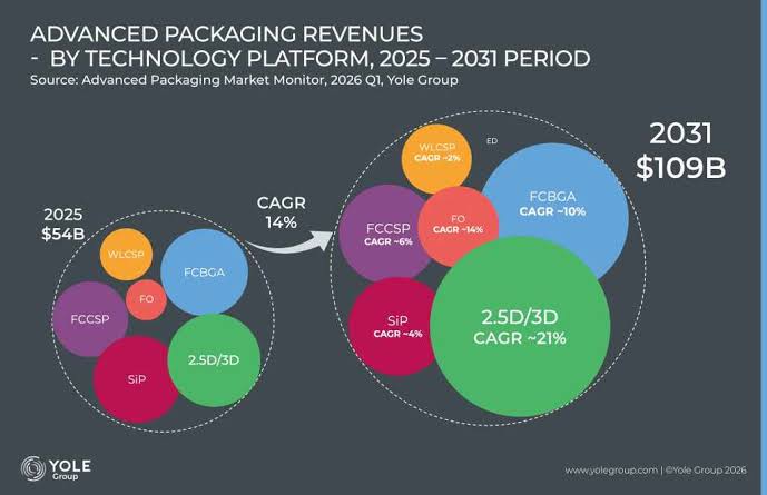
Yole's data confirms this transformation. The organization predicts that the global advanced packaging market will grow at a compound annual growth rate (CAGR) of 9.4%, with a market size of nearly $80 billion by 2030. Recently, this forecast has been further raised to over $109 billion. Driven by the demand for AI and data centers, the 2.5D/3D advanced packaging market is rapidly expanding, with an expected market size of nearly $35 billion by 2030 and a CAGR of approximately 19% from 2024 to 2030. Morgan Stanley predicts that the scale of China's advanced packaging market will reach the level of billions of yuan by 2029.
The Transformation of Packaging Technology under the Wave of AI
Driven by the wave of AI, 2.5D/3D has become the key to continuing the development of the industry. TSMC's 2.5D platform CoWoS has evolved into three variants: CoWoS-S, CoWoS-L, and CoWoS-R. Oversized packaging faces the challenge of warping: the maximum size of the CoWoS-S intermediate layer is 3.3X Reticle, and the maximum size of the CoWoS-R mass-produced layer is 4X Reticle. Exceeding the limit will result in warping and loss of control; CoWoS-L has pushed the maximum size to 9.5X Reticle through Bridge die technology, becoming a demand trend.
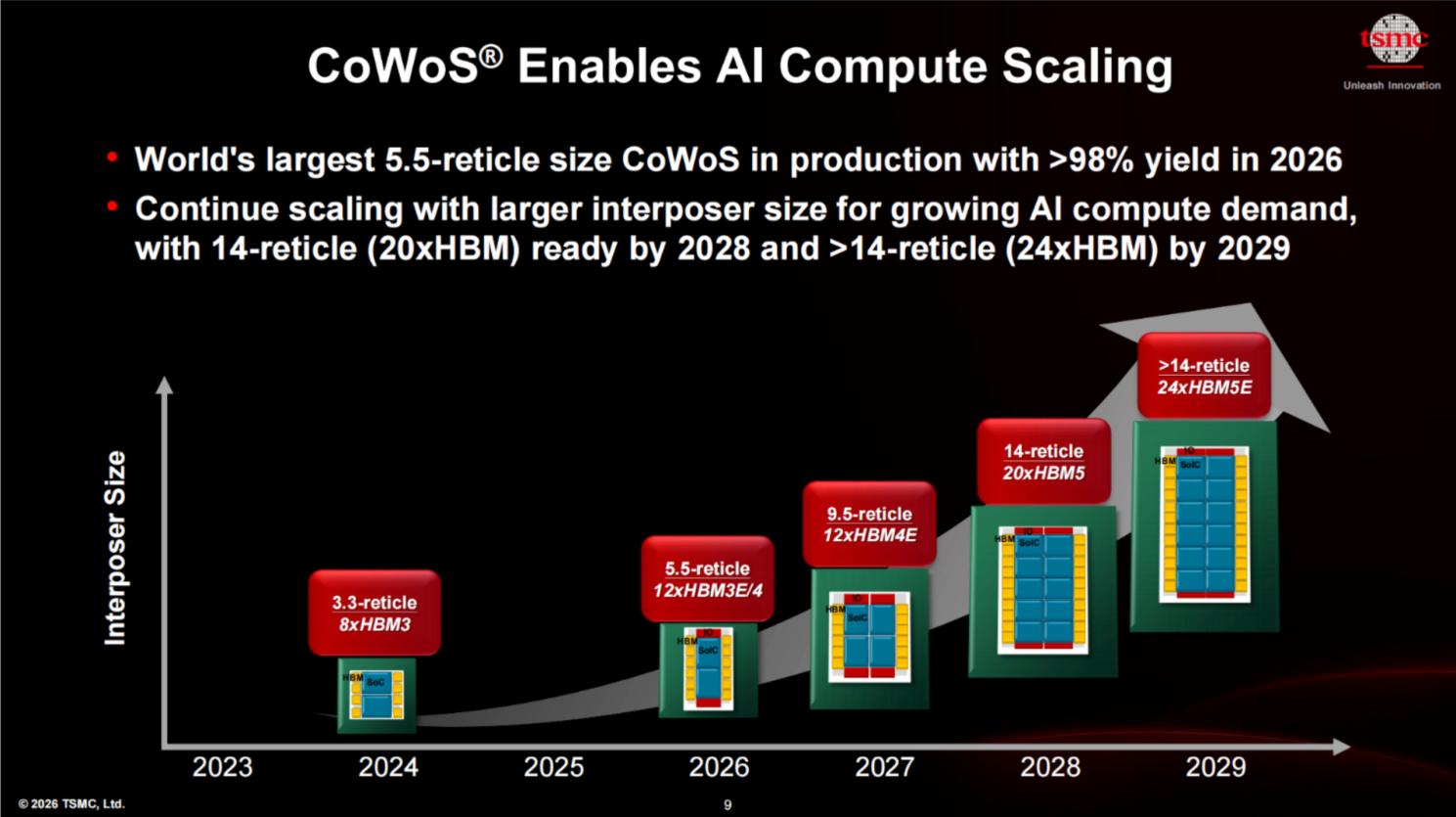
TSMC is expanding the size of silicon interlayer and increasing HBM integration to achieve leapfrog development. The 2026 technical seminar route shows that starting from 3.3X (8 HBM3) in 2024, the world's largest 5.5X (12 HBM3E/4) will be mass-produced in 2026, with a yield rate of over 98%. It is planned to reach 14X in 2028 and break through to above 14X in 2029.
As the chip size increases, the bottleneck of circular wafer area utilization becomes apparent. TSMC regards panel level CoWoP and CoPoS as cutting-edge alternatives to CoWoS; Technologies such as CPO and NPO are also approaching mass production.
The threshold for advanced packaging is much higher than that of traditional packaging and testing, and the barriers of process, yield, and cost make competition a platform based war for top players: the first tier includes wafer fabs such as TSMC and Samsung; The second tier consists of international testing giants such as Riyueguang and Ankao; The third echelon is Shenghe Jingwei, Changdian, Tongfu, Huatian and other manufacturers in Chinese Mainland, which are still catching up. The intensive launch of new AI chip products in China has led to an urgent demand for local high-end packaging capacity, but the supply is still relatively limited.
Huatian Advanced eSinC Platformization Path
Faced with industry challenges such as intermediate layer processes, core equipment, yield ramp up, and capacity supply, as the third largest packaging and testing enterprise in China and the fifth largest in the world, Huatian Technology chooses to benchmark global leading solutions and build a complete process platform, committed to building high-end packaging into a "stable and obtainable production capacity".
The company has invested a total of 34 billion yuan to carry out layout with four advanced sealing and testing bases. Among them, Nanjing Huatian Advanced Packaging Co., Ltd. (Huatian Advanced) is the core carrier for tackling 2.5D/3D packaging, with a total investment of 2 billion yuan, and has completed the production line in the fourth quarter of 2024.
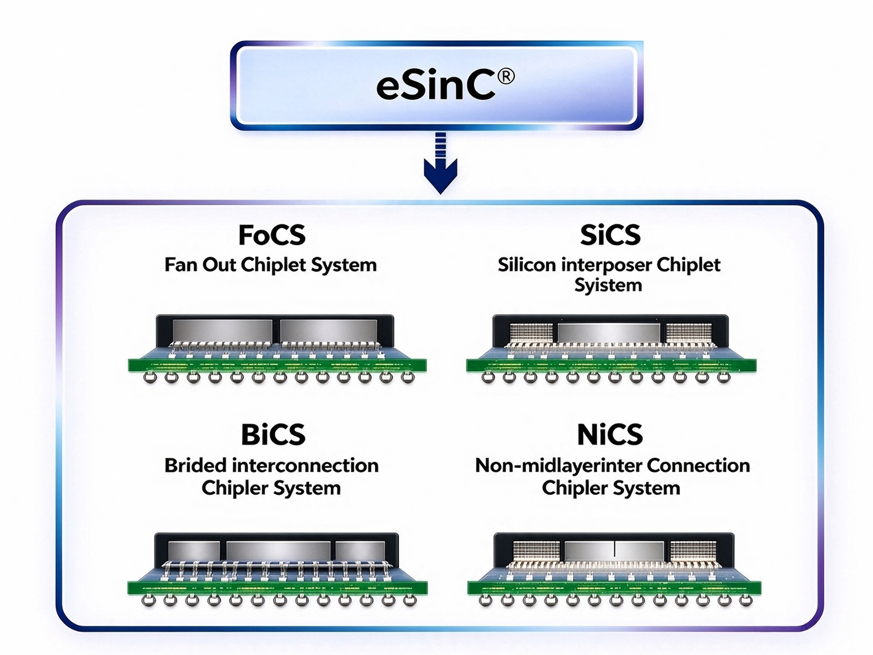
In response to the demands of the AI era, Huatian has advanced the development of the eSinC (Embedded System in Chip) 2.5D packaging platform, using independent and controllable processes to bridge the "last mile" of high-end computing chips landing. The platform includes three technical routes: FoCS benchmarking CoWoS-R and adopting RDL middleware; SiCS benchmarks CoWoS-S and uses a silicon intermediate layer; BiCS is benchmarked against CoWoS-L and uses an embedded silicon bridge.
The difference among the three lies in the trade-off between performance and size: SiCS has the best interconnect performance but is constrained by warpage; FoCS has lower cost and better resistance to warping, but its interconnect density is limited; BiCS embeds silicon bridges in critical signal paths and uses RDL for the rest, balancing performance and cost.
The eSinC platform is evolving along the path of reducing micro bump spacing, miniaturizing RDL line width and spacing, and enlarging package size. At present, SiCS is in small batch production and has achieved a 40um micro bump spacing and 1.3X retaining, while FoCS has achieved a 2/2um RDL and 45um micro bump spacing; The BiCS under development can achieve a spacing between 5/5um RDL and 40um micro bumps. The sample delivery is planned to be completed by the end of the year, and the size will be pushed to 5.5X Reticle and larger.
Relying on the complete 2.5D process development chain, the company synchronously provides supporting engineering capabilities such as high-density micro bumps, high-precision bonding, wafer level plastic packaging, large-sized high-speed substrates, system level thermal simulation and reliability verification, etc., filling in the full process supporting links of heterogeneous integration, and providing customers with integrated development services from AB0-AB1-AB2-FT full packaging and testing. At the same time, based on the 2.5D platform, new packaging solutions such as FOPoP and CPO can be extended, and customized process development can be carried out in combination with market demand and customer projects.
Conclusion
The rapid development of the AI industry continues to amplify the demand for high computing power chips and HBMs. The tight supply and demand of 2.5D/3D packaging is difficult to solve in the short term. The global advanced packaging market is expanding at the level of billions of dollars, and the Chinese market is expected to reach the level of billions of dollars by 2029. In this context, the focus of competition is shifting towards mass production certainty and customer response speed. Huatian Advanced is advancing along this path, striving to become a key link in the process of advanced packaging moving from "scarce production capacity" to "stable supply" in the local high-end packaging and testing industry.
